TSMC Symposium 2024

TSMC's 3D-stacked system-on-integrated chips (SoIC) advanced packaging technologies is set to evolve rapidly. In a presentation at the company's recent technology symposium, TSMC outlined a roadmap that will take the technology from a current bump pitch of 9μm all the way down to a 3μm pitch by 2027, stacking together combinations of A16 and N2 dies. TSMC has a number of advanced packaging technologies, including 2.5D CoWoS and 2.5D/3D InFO. Perhaps the most intriguing (and complex) method is their 3D-stacked system-on-integrated chips (SoIC) technology, which is TSMC's implementation of hybrid wafer bonding. Hybrid bonding allows two advanced logic devices to be stacked directly on top of each other, allowing for ultra-dense (and ultra-short) connections between the two chips, and is primarily aimed at high performance...
TSMC: Performance and Yields of 2nm on Track, Mass Production To Start In 2025
In addition to revealing its roadmap and plans concerning its current leading-edge process technologies, TSMC also shared progress of its N2 node as part of its Symposiums 2024. The...
4 by Anton Shilov yesterday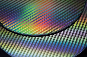
TSMC's Roadmap at a Glance: N3X, N2P, A16 Coming in 2025/2026
As announced last week by TSMC, later this year the company is set to start high-volume manufacturing on its N3P fabrication process, and this will be the company's most...
46 by Anton Shilov on 5/22/2024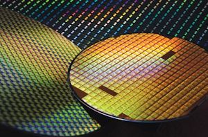
TSMC Offers a Peek at 'Global Gigafab' Process Replication Program
At its European Technology Symposium last week TSMC revealed some of the details about its Global Gigafab Manufacturing program, the company's strategy to replicate its manufacturing processes across its...
11 by Anton Shilov on 5/22/2024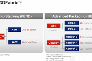
TSMC to Expand CoWoS Capacity by 60% Yearly Through 2026
Customer demand for AI and HPC processors is driving a much greater use of advanced packaging technologies, particularly TSMC's chip-on-wafer-on-substrate (CoWoS) services. As things stand, TSMC is just barely...
8 by Anton Shilov on 5/21/2024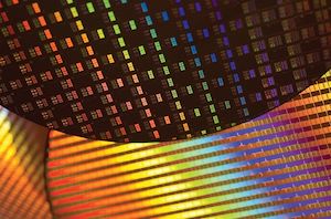
TSMC Outlines Path to EUV Success: More Tools, More Wafers, & Best Pellicles In Industry
Although TSMC can't claim to be the first fab to use extreme UV (EUV) lithography – that title goes to Samsung – they do get to claim to be...
20 by Anton Shilov on 5/17/2024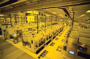
TSMC to Expand Specialty Capacity by 50%, Introduce 4nm N4e Low-Power Node
With all the new fabs being built in Germany and Japan, as well as the expansion of production capacity in China, TSMC is planning to extend its production capacity...
0 by Anton Shilov on 5/16/2024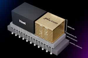
TSMC Readies Next-Gen HBM4 Base Dies, Built on 12nm and 5nm Nodes
Of the several major changes coming with HBM4 memory, one of the most immediate is the sheer width of the memory interface. With the fourth-generation memory standard moving from...
1 by Anton Shilov on 5/16/2024
TSMC: Performance-Optimized 3nm N3P Process on Track for Mass Production This Year
As part of the second leg of TSMC's spring technology symposium series, the company offered an update on the state of its 3nm-class processes, both current and future. Building...
21 by Anton Shilov on 5/15/2024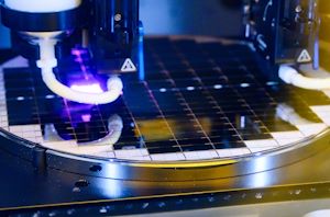
TSMC Readies 8x Reticle Super Carrier Interposer For Next-Gen Chips Twice as Large As Today's
TSMC is no stranger to building big chips. Besides the ~800mm2 reticle limit of their normal logic processes, the company already produces even larger chips by fitting multiple dies...
6 by Anton Shilov on 4/30/2024
TSMC Jumps Into Silicon Photonics, Lays Out Roadmap For 12.8 Tbps COUPE On-Package Interconnect
Optical connectivity – and especially silicon photonics – is expected to become a crucial technology to enable connectivity for next-generation datacenters, particularly those designed HPC applications. With ever-increasing bandwidth...
9 by Anton Shilov on 4/26/2024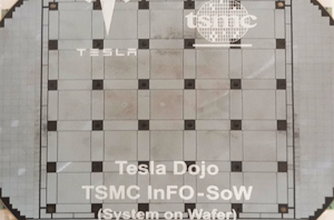
TSMC's System-on-Wafer Platform Goes 3D: CoW-SoW Stacks Up the Chips
TSMC has been offering its System-on-Wafer integration technology, InFO-SoW, since 2020. For now, only Cerebras and Tesla have developed wafer scale processor designs using it, as while they have...
2 by Anton Shilov on 4/26/2024
TSMC Preps Cheaper 4nm N4C Process For 2025, Aiming For 8.5% Cost Reduction
While the bulk of attention on TSMC is aimed at its leading-edge nodes, such as N3E and N2, loads of chips will continue to be made using more mature...
6 by Anton Shilov on 4/25/2024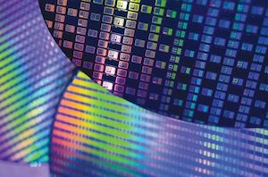
TSMC 2nm Update: N2 In 2025, N2P Loses Backside Power, and NanoFlex Brings Optimal Cells
Taiwan Semiconductor Manufacturing Co. provided several important updates about its upcoming process technologies at its North American Technology Symposium 2024. At a high level, TSMC's 2 nm plans remain...
0 by Anton Shilov on 4/25/2024
TSMC's 1.6nm Technology Announced for Late 2026: A16 with "Super Power Rail" Backside Power
With the arrival of spring comes showers, flowers, and in the technology industry, TSMC's annual technology symposium series. With customers spread all around the world, the Taiwanese pure play...
18 by Anton Shilov on 4/25/2024


