The Era of Tera: Intel Reveals more about 80-core CPU
by Anand Lal Shimpi on February 11, 2007 5:44 PM EST- Posted in
- CPUs
With no Spring Intel Developer Forum happening this year in the US, we turn to the International Solid-State Circuits Conference (ISSCC) for an update on Intel's ongoing R&D projects. Normally we'd hear about these sorts of research projects on the final day of IDF, these days presented by Justin Rattner, but this year things are a bit different. The main topic at hand today is one of Intel's Tera-scale computing projects, but before we get to the chip in particular we should revisit the pieces of the puzzle that led us here to begin with.
Recapping Tera-Problems
At the Spring 2005 Intel Developer Forum, Justin Rattner outlined a very serious problem for multi-core chips of the future: memory bandwidth. We're already seeing these problems today, as x86 single, dual and quad core CPUs currently all have the same amount of memory bandwidth. The problem becomes even more severe when you have 8, 16, 32 and more cores on a single chip.
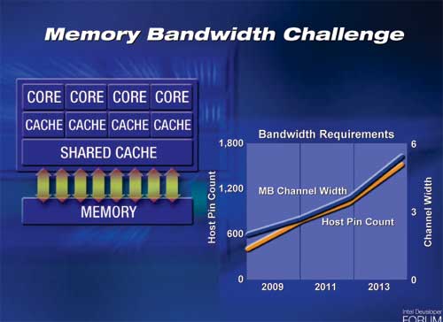
The obvious solution to this problem is to use wider front side and memory buses that run at higher frequencies, but that solution is only temporary. Intel's slide above shows that a 6-channel memory controller would require approximately 1800 pins, and at that point you get into serious routing and packaging constraints. Simply widening the memory bus and relying on faster memory to keep up with the scaling of cores on CPUs isn't sufficient for the future of microprocessors.
So what do you do when a CPU's access to data gets slower and more constrained? You introduce another level in the memory hierarchy of course. Each level of the memory hierarchy (register file, L1/L2/L3 cache, main memory, hard disk) is designed to help mask the latency of accessing data at the level immediately below it. The clear solution to keeping massively multi-core systems fed with data then is to simply put more memory on die, maybe an L4 cache perhaps?
The issue you run into here is that CPU die space is expensive, and the amount of memory we'd need to keep tens of cores fed is more than a few megabytes of cache can provide. Instead of making the CPU die wider, Intel proposed to stack multiple die on top of each other. A CPU die, composed of many cores, would simply be one layer in a chip that has integrated DRAM or Flash or both. Since the per-die area doesn't increase, the number of defects don't go up per die.
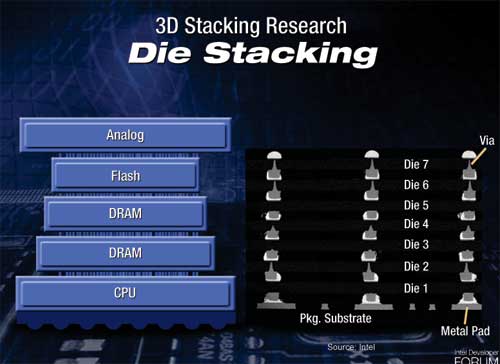
Memory bandwidth improves tremendously, as your DRAM die can have an extremely wide bus to connect directly to your CPU cores. Latency is also much improved as the CPU doesn't have to leave the package to get data stored in any of the memory layers.
Obviously there will still be a need for main memory, as Intel is currently estimating that a single layer could house 256MB of memory. With a handful of layers, and a reasonably wide external memory bus, keeping a CPU with tens of cores fed with data now enters the realm of possibility.
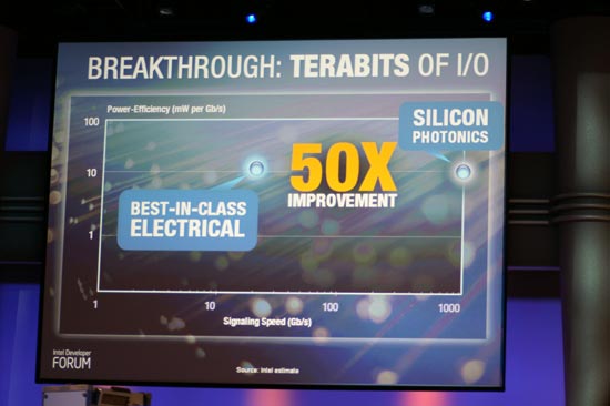
A year and a half later, Rattner was back but this time he was tackling another aspect of the era of tera - bus bandwidth. Although 3D die stacking will help keep many cores on a single die fed with data, the CPU still needs to communicate with the outside world. FSB technology, especially from Intel, has remained relatively stagnant over the past several years. If we're talking about building CPUs with tens of cores, not only will they need tons of memory bandwidth but they'll also need a very fast connection to the outside world.
Intel's research into Silicon Photonics has produced a functional hybrid silicon laser demonstrated at the Intel Developer Forum late last year. The idea is that optical buses can offer much better signaling speed and power efficiency than their electrical equivalents, resulting in the ideal bus for future massively multi-core CPUs.
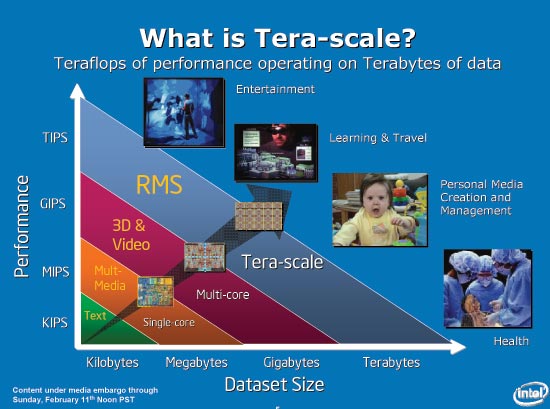
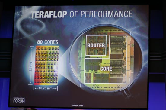
Justin Rattner's keynotes talked about some of Intel's Tera-scale projects, with 3D die stacking delivering terabytes of bandwidth needed for the next decade of CPUs and silicon photonics enabling terabits of I/O for connecting these CPUs to the rest of the system. The final vector that Rattner spoke about, was delivering a teraflop of performance. The CPU Rattner spoke of was a custom design by Intel that featured 80 cores on a single die, and today Intel revealed a lot more about its Teraflop CPU, the architecture behind it and where it fits in with the future of Intel CPUs.


25 Comments
View All Comments
creathir - Monday, February 12, 2007 - link
With all of this wonderful multi-core bliss, is the software side of things. Multicore means the software needs to be written asymentrically. This will be an incredibly hard challenge, especially on real time applications such as video games. The concept is fantastic, but the proof is in the pudding as they say. I do find Intel's routing technology to be quite interesting, especially the idea of stacking the L1/L2 memory on top (or below rather;)) the cores. The interconnect on them, how would this work exactly I wonder? Should be interesting to see what all 3 of these companies come out with in the coming years. I suppose the nay sayers of Moore's law will be once again disproven...- Creathir
Goty - Sunday, February 11, 2007 - link
So basically it's a Cell processor on steroids. Other than the chip stacking, what's so new about it? People have been talking about 3D packaging for a year or two now, and not just Intel.SocrPlyr - Monday, February 12, 2007 - link
In a way, yes. And in a lot of ways, no. Yes the individual tiles are floating point units, but this chip is not meant to be a functional replacement for anything like the cell is trying to be. You really cannot compare this chip to anything available on the market. It is only a proof of concept. The choice of tiles that are floating point units was probably due to the fact that ultra high performance needs generally are nearly completely FP dependent. When testing and playing with this thing those types of applications are easy to come by. To be honest this chip seems a lot like a DSP chip, and mentioning those you will realize that the Cell processor is anything but an altered one of those. Really on all sides there has been little technology that is completely new, just better implementations.oldhoss - Sunday, February 11, 2007 - link
I'll bet that SOB would give two 8800GTX's a run for their money....CPU-limited be damned! ;-Dmino - Sunday, February 11, 2007 - link
"Since the per-die area doesn't increase, the number of defects don't go up per die."Any sensible person knows that defect-rate is(mostly) dependent on the number of functional units(i.e. transistors), provided the defect-rate off a single unit is set.
The fact that it is NOW mostly tied to die-area is caused exactly by the fact we do NOT use stacked-die aproach yet.
Otherwise a nice news piece. Thanks AT.
mino - Sunday, February 11, 2007 - link
sorry for typpos...notposting - Sunday, February 11, 2007 - link
The picture above this shows the Terascale slide:
http://images.anandtech.com/reviews/cpu/intel/tera...">http://images.anandtech.com/reviews/cpu/intel/tera...
sprockkets - Sunday, February 11, 2007 - link
We have a solution to the problem of ever increasing CPU speed. My question is, who here needs it?For those who need to open 80 Firefox tabs, video encoding, virus scanning and watching a HD movie, at the same time?
Data sets did need to get bigger, but check this out: Music files started out at small sampling rates till about Win98 they got to the cd standard. It stopped there since no one needs it bigger than that, that is, 44.1khz and 16 bit resolution. If you can hear 96/192khz 24bit music better, fine, but we have others saying that 128kbps mp3 was cd quality.
Video resolutions made their way from 640x480 to now around 1600x1200, and widescreen varients of that. Color depth sits at around 32bit. Can you see it improving beyond that?
OK, so we can what, go 3D now, holographic?
Sorry to you Intel and AMD, but the vast majority of the people you sell your technology to can live off a $30 processor and $50 of RAM, the smallest HDD, and a $30 optical drive which does everything.
Would be cool to see a motherboard with built in DDR3 or 4 memory for the cpu/gpu AMD Fusion core, and have 2GB of it, with 32GB of flash built on as well. Let's go for silent computing, you know, back in the day when all processors only had tiny heatsinks on them!!!
joex444 - Monday, February 12, 2007 - link
What part of the article was confusing to you?NOT FOR RETAIL SALE, COMMERCIAL USES ONLY.
I got the idea, guess you didn't. PWNT!
Larso - Monday, February 12, 2007 - link
So, why did we ever bother invent plastic materials? Or why invent the laser? The laser is a good example of an invention that was expected to be a useless curiosity but turned out to be hugely usefull.But this case isn't even comparable to that. There are indeed problems waiting to be solved with this solution. All servers with more than a handfull of CPU's could be cut down in size and power usage tremendously, and what about supercomputers? They are going to be extra extremely powerfull when they change to this kind of cpu's.
And by the way, you have to be quite narrowminded to not see the (sales) potential of supercomputing at home. Lets have computer games with scary intelligent AI's :)