NVIDIA's 1.4 Billion Transistor GPU: GT200 Arrives as the GeForce GTX 280 & 260
by Anand Lal Shimpi & Derek Wilson on June 16, 2008 9:00 AM EST- Posted in
- GPUs
Tweaks and Enahancements in GT200
NVIDIA provided us with a list, other than the obvious addition of units and major enhancements in features and technology, of adjustments made from G80 to GT200. These less obvious changes are part of what makes this second generation Tesla architecture a well evolved G80. First up, here's a quick look at percent increases from G80 to GT200.
| NVIDIA Architecture Comparison | 8800 GTX | GTX 280 | % Increase |
| Cores | 128 | 240 | 87.5% |
| Texture | 64t/clk | 80t/clk | 25% |
| ROP Blend | 12p / clk | 32p / clk | 167% |
| Max Precision | fp32 | fp64 | |
| GFLOPs | 518 | 933 | 80% |
| FB Bandwidth | 86 GB/s | 142 GB/s | 65% |
| Texture Fill Rate | 37 GT/s | 48 GT/s | 29.7% |
| ROP Blend Rate | 7 GBL/s | 19 GBLs | 171% |
| PCI Express Bandwidth | 6.4 GB/s | 12.8GB/s | 100% |
| Video Decode | VP1 | VP2 |
Communication between the driver and the front-end hardware has been enhanced through changes to the communications protocol. These changes were designed to help facilitate more efficient data movement between the driver and the hardware. On G80/G92, the front-end could end up in contention with the "data assembler" (input assembler) when performing indexed primitive fetches and forced the hardware to run at less than full speed. This has been fixed with GT200 through some optimizations to the memory crossbar between the assembler and the frame buffer.
The post-transform cache size has been increased. This cache is used to hold transformed vertex and geometry data that is ready for the viewport clip/cull stage, and increasing the size of it has resulted in faster communication and fewer pipeline stalls. Apparently setup rates are similar to G80 at up to one primative per clock, but feeding the setup engine is more efficient with a larger cache.
Z-Cull performance has been improved, while Early-Z rejection rates have increased due to the addition of more ROPs. Per ROP, GT200 can eliminate 32 pixles (or up to 256 samples with 8xAA) per clock.
The most vague improvement we have on the list is this one: "significant micro-architectural improvements in register allocation, instruction scheduling, and instruction issue." These are apparently the improvements that have enabled better "dual-issue" on GT200, but that's still rather vague as to what is actually different. It is mentioned that scheduling between the texture units and SMs within a TPC has also been improved. Again, more detail would be appreciated, but it is at least worth noting that some work went into that area.
Register Files? Double Em!
Each of those itty-bitty SPs is a single-core microprocessor, and as such it has its own register file. As you may remember from our CPU architecture articles, registers are storage areas used to directly feed execution units in a CPU core. A processor's register file is its collection of registers and although we don't know the exact number that were in G80's SPs, we do know that the number has been doubled for GT200.
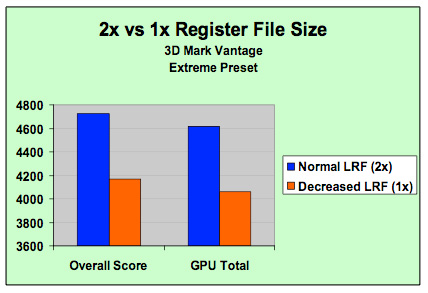
NVIDIA's own data shows a greater than 10% increase in performance due to the larger register file size (source: NVIDIA)
If NVIDIA is betting that games are going to continue to get more compute intensive, then register file usage should increase as well. More computations means more registers in use, which in turn means that there's a greater likelihood of running out of registers. If a processor runs out of registers, it needs to start swapping data out to much slower memory and performance suffers tremendously.
If you haven't gotten the impression that NVIDIA's GT200 is a compute workhorse, doubling the size of the register file per SP (multiply that by 240 SPs in the chip) should help drive the idea home.
Double the Precision, 1/8th the Performance
Another major feature of the GT200 GPU and cards based on it is support for hardware double precision floating point operations. Double precision FP operations are 64-bits wide vs. 32-bit for single precision FP operations.
Now the 240 SPs in GT200 are single-precision only, they simply can't accept 64-bit operations at all. In order to add hardware level double precision NVIDIA actually includes one double precision unit per shading multiprocessor, for a total of 30 double precision units across the entire chip.
The ratio of double precision to single precision hardware in GT200 is ridiculously low, to the point that it's mostly useless for graphics rasterization. It is however, useful for scientific computing and other GPGPU applications.
It's unlikely that 3D games will make use of double precision FP extensively, especially given that 8-bit integer and 16-bit floating point are still used in many shader programs today. If anything, we'll see the use of DP FP operations in geometry and vertex operations first, before we ever need that sort of precision for color - much like how the transition to single precision FP started first in vertex shaders before eventually gaining support throughout the 3D pipeline.
Geometry Wars
ATI's R600 is alright at geometry shading. So is RV670. G80 didn't really keep up in this area. Of course, games haven't really made extensive use of geometry shaders because neither AMD nor NVIDIA offered compelling performance and other techniques made more efficient use of the hardware. This has worked out well for NVIDIA so far, but they couldn't ignore the issue forever.
GT200 has enhanced geometry shading support over G80 and is now on par with what we wish we had seen last year. We can't fault NVIDIA too much as with such divergent new features they had to try and predict the usage models that developers might be interested in years in advance. Now that we are here and can see what developers want to do with geometry shading, it makes sense to enhance the hardware in ways that support these efforts.
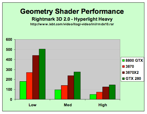
GT200 has significantly improved geometry shader performance compared to G80 (source: NVIDIA)
Generation of vertex data is a particularly weak part of NVIDIA's G80, so GT200 is capable of streaming out 6x the data of G80. Of course there are the scheduling enhancements that affect everything, but it is unclear as to whether NVIDIA did anything beyond increasing the size of their internal output buffers by 6x in order to enhance their geometry shading capability. Certainly this was lacking previously, but hopefully this will make heavy use of the geometry shader something developers are both interested in and can take advantage of.


108 Comments
View All Comments
woofermazing - Tuesday, June 17, 2008 - link
Isn't the R700 high-end model going to have a direct link between the two cores. Could be a false rumor, but i would think that would solve a lot of problems with having two GPU's on a single board, since games would see it as 1 chip instead of a Crossfire/SLI setup. And besides, why the heck does it matter what the card looks like under the cooler. If it delivers better performance than Nvidia's offering without driver headaches, I don't think most gamers are going to care.VooDooAddict - Tuesday, June 17, 2008 - link
Why am I the only one happy about this product?Since the release of the 8800GTX top end single GPU performance has been a little stagnant... then came the refresh (8800GT/8800GTS-512) better prices came into effect.
Now we've got the new generation, and like in years prior, the new gen single GPU card has near performance of the previous gen in SLI. Price is also similar with when NVIDIA launched the first 8800GTX.
Sure, I wish they came in at a lower price point and at less power draw. (Same complaints that we had with the original 8800GTX). Lower power and lower price will come with a refresh.
Will I be getting one? ... nahh these cheap 9600GTs, overclocked 8800GT's and 8800GTSs will be the cards I recomend till i see the refresh. But I'm still happy there's progress.
I'm hoping the refresh hits around the same time as Intel's updated quad core.
DerekWilson - Tuesday, June 17, 2008 - link
i think its neat and has very interesting technology under the hood.but i'm not gonna spend that much money for something that doesn't deliver enough value (or even performance) compared to other solutions that are available. you pretty much reflect my own sentiment there: it's another step forward but not one that you're gonna buy.
i think people "don't like it" because of that though. it just isn't worth it right now and that's certainly valid.
greenx - Tuesday, June 17, 2008 - link
There are two ways I can look at this article.1)First an foremost at the heart of a real gamer ticks the need for good story lines fed by characters you will never forget, held by a gameplay you will fall in love with and finally covered by graphics that will transport you to another world (kinda like when I first played FF VII on my PC).
Within the context of the world we live in today I wonder what is really going through the minds of these people selling $600+ video cards. Kinda like those $10 000+ PCs. Madness. Sure they have their market up there but I shudder to think of how much money has been poured into appeasing a select few. Furthermore for what reason? Glory? I don't know but seeing as how the average gamer is what has made the PC/Gaming scene what it is, where does a $600+ video card fit into the grand scheme of things?
2) The possibilities that these new cards open up certainly seem exciting. The comparison with intel has been justified, but considering the other alternatives out there are much further ahead in development, who is going to bypass intel/amd/etc for a GPU technology based supercomputer?
DerekWilson - Tuesday, June 17, 2008 - link
two address point 2):developers will bypass Intel, AMD, SUN, whoever owns Cray these days, and all other HPC developers when a technology comes along that can speed up their applications by two orders of magnitude immediately on hardware that costs thousands (and in large cases millions) less to build, run and develop for.
evolucion8 - Tuesday, June 17, 2008 - link
LOL that was quite funny but incorrect as well, there's more than 4 Billion of people in China, in the future probably nVidia will launch a 4 Billion Transistors GPU hehe. It will require a Nuclear Reactor to turn it on, a and two of them to play games :D7Enigma - Wednesday, June 18, 2008 - link
4 Billion? Did you just make that out of thin air. Latest tabs show approximately 1.4 billion (give or take a couple hundred million). The world population is only estimated at 6.6 billion, so unless 60% of the people in the world are living in China, you're clueless.http://geography.about.com/od/populationgeography/...">http://geography.about.com/od/populationgeography/...
Bahadir - Tuesday, June 17, 2008 - link
Firstly I must say I enjoyed reading the whole article written by Anand Lal Shimpi & Derek Wilson. However, what does not make sense to me is the fact that "At most, 105 NVIDIA GT200 die can be produced on a single 300mm 65nm wafer from TSMC", but by looking at the wafer, only 95 full dies can be seen. Is this the wrong die?Also, it is not fair to compare the die of the Penryn against the GTX 280die because Penryn's die was made in 45nm process and GTX280 was made in 65nm die. Maybe it would be fair to compare it with the Conroe (65nm) die. But well done folks for putting an excellent article together!
Anand Lal Shimpi - Tuesday, June 17, 2008 - link
Thanks for your kind words btw :) Both of us really appreciate it - same to everyone else in this thread, thanks for making a ridiculously long couple of weeks (and a VERY long night) worth it :)-A
Anand Lal Shimpi - Tuesday, June 17, 2008 - link
You're right, there's actually a maximum of 94 usable die per wafer :)Take care,
Anand