EVGA X58 Classified - First Look
by Rajinder Gill on February 27, 2009 5:00 AM EST- Posted in
- Motherboards
EVGA's Classified X58 motherboard has been a centerpiece of X58 discussions in various forums since the start of 2009. We managed to get an engineering sample board a few weeks ago and have some initial overclocking tests to show today. Let's take a quick look at the current layout and features before we have a look at a few early benchmark runs.


Our board arrived before EVGA finalized the stock cooling design, so we have had to resort to using third party solutions to cool areas of the board for these initial test runs. We are waiting on a retail board from EVGA before we comment on thermal performance and power consumption.
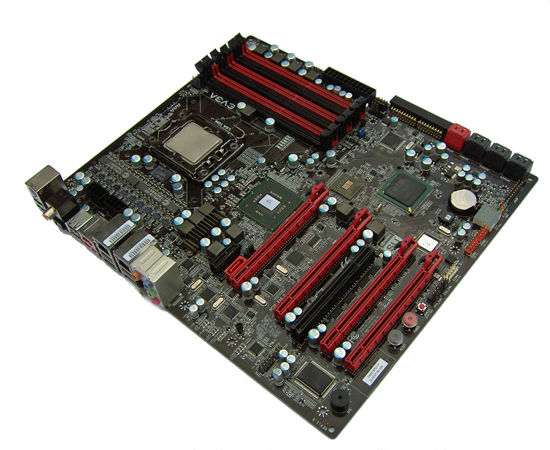
Hardware wise, EVGA added NVIDIA's NF200 into the mix that allows four x16 electrical interface PCI-E slots. As many of you already know, the NF200 is a PCI-E 2.0 x16 bridge-chip solution, which does add extra latency to the data transfer process. However, that's not a huge issue in the overall package.
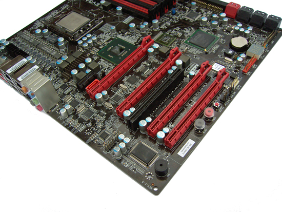
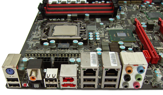
This board is set to become EVGA's flagship board by offering a slew of extreme overclocking friendly features. This holds true for the 10-phase Volterra CPU power, 3-phase memory power, and 3-phase VTT designs to onboard jumpers that override cold boot quirks for LN2 cooling. The product focus is squarely aimed at multi-GPU enthusiasts and those that benchmark more for competition than fun. The slot configuration allows running three dual slot GPUs and a single slot PhysX card or other PCI-E peripheral. A PCI-E x1 slot is available for audio duties, even if the GPU slots are completely loaded.
This board is clearly for those with deep, deep pockets. The launch price is expected to be around $400~$450, putting it off the radar for most. EVGA provides a plug-in remote PCB, supporting power, reset, CMOS clear, a hex POST code LED display, on-the-fly VCore adjustment, and PCI-E disable jumpers. The remote buttons come in handy when benchmarking the board out of a PC case, especially when the lowest PCI-E slot is occupied.
A new addition that EVGA just completed for the final retail board is the presence of an onboard ROM that can store memory SPD files. The user can select at BIOS POST to override the memory module base SPD. EVGA has developed an OS software tool that allows users to interchange SPDs with one another if a particular SPD file known to offer superlative performance for a memory chip/PCB combination is available. Our test board does not contain this technology, so we will have to wait for the arrival of our retail board to test this unique feature.
We have been throwing everything we can at the board using the latest test BIOS. So far, things have been smooth during the test process, mainly because the EVGA X58 SLI board's launch has provided insight to the EVGA team and us in getting this board up and operating quickly. Peripheral compatibility has been excellent on this board. We have not discovered a single device that was not recognized or refused to work properly. S3 resume states have worked for us all the way up to 215 BCLK (as far as we tested to date), which cures a problem on the X58 SLI board.
Unfortunately, we still do not have an official release date from EVGA, but we expect it sometime in March (subject to change, obviously). At stock speeds, this board offers similar performance to other X58 motherboards in a variety of applications and games. Our short preview today will cover SLI gaming performance to see if the NF200 is a handicap and a few overclocking results using subzero and water-cooling, which is relevant as this board is targeted at the competitive overclocking crowd.
We are also providing a descriptive analysis of the BIOS overclocking options and how they work not only on this board but also on the X58 platform in general. We will follow up with a revised BIOS guide when the board launches. In the meantime, let's take a quick look at our results today.


22 Comments
View All Comments
rogguy - Thursday, March 12, 2009 - link
this board is mediocre compared to asus ROGEverlong19 - Thursday, March 12, 2009 - link
How can you have a triple GPU setup using dual slot cards and have room for a physics card/sound card?Only way it might be possible is putting the 3rd card in the 4th PCI-E slot, but that would overlap the USB headers etc. The PCI slot gets covered by the 2nd GPU, so any PCI sound cards can't go in there, either.
MadMan007 - Saturday, February 28, 2009 - link
The important thing I take away from this preview has nothing to do with the board itself but rather eVGA's expanding custom software and software/hardware efforts. It's really neat to see a company like eVGA make a push in this direction going well beyond other mobo companies with their basic monitoring software and other graphics rebadgers.MasonStorm - Saturday, February 28, 2009 - link
You could certainly do it, as stated, by plugging one of the dual-slot cards into that last slot, and having it hang over the edge of the board - requiring an extra big case. But another way is to use liquid-cooled versions of the cards, cutting them all down to single-slot size. In any event, it doesn't matter where you place them, since you can use three of the soft, bendy SLI bridge connectors to make your own triple-SLI connection. You don't have to use anybody's firm, fixed triple-SLI connector. Just Google around to see how to use the three individual, soft, bendy connectors.Casper42 - Friday, February 27, 2009 - link
Question on this comment:The slot configuration allows running three dual slot GPUs and a single slot PhysX card or other PCI-E peripheral
In looking at the pictures, this board only has 7 slots total with the x1 being at the top.
If you used 3 Dual Slot GPUs, that would be 3 x 2 = 6 + the x1 = 7
So where exactly are you putting a PhysX card?
The only possibility I see is if you use an 8 or 10 slot Case and stick the 3rd Dual Slot GPU in the very bottom slot such that it hangs off the bottom of the mobo. But in this case, the normal 6 connector Triple SLI Bridge wont reach the 3rd card.
Am I missing something here?
PS: Dont get me wrong, I like the design of the board.
Rajinder Gill - Friday, February 27, 2009 - link
You are right the 3rd SLI card would go in the last PCIe slot, with a dual card overhanging. An SLI bridge supporting this will ship with the retail board.Board dimensions are 310mmX265mm btw. Big case territory.
regards
Raja
cesthree - Friday, February 27, 2009 - link
Remember the awesome 7X0i series of motherboards? Especially the last one with the NF200 on it? It's called a 790i "Ultra" chipset.There are only a few people who ever had problems with the 7X0i series motherboards when using multiple GPU's. Not one person ever complained about things like "freezing" or "hard locking" or "data corruption." Especially not at stock speeds.
Just like there is absolutely no sarcasm in my last paragraph.
What fool would by the "Classified" EVGA motherboard? It's got negligible performance increases. Why go through that much trouble for all of the 5 people on earth who would purchase it and use it with 3-4 GPU's + 30" or bigger monitor.
Mark my words. The NF200 addition to the X58 that EVGA already had going GREAT for them, will bring them problems on the level with the last batch of shoddy, Nvidia tainted motherboards.
I am going to put this in all my sigs from now on:
"Nvidia, for the love of god, please stop crippling motherboards and just stick to GPU's."
Von Matrices - Friday, February 27, 2009 - link
From what I can tell from sources online, the NF200 bridges 16 PCIe 1.1 lanes to 32 PCIe 2.0 lanes. What is there to gain by using the NF200 over just using four PCIe x8 2.0 lanes of bandwidth from the IOH? With the NF200, you get ~4GB/s bandwidth to the IOH per graphics slot compared to ~8GB/s with a native solution, and the bridge adds additional latency, which further reduces performance, and additional cost. Why would EVGA use it then? Are there any advantages to it?Zak - Friday, February 27, 2009 - link
Question. 920 can be easily o/clocked on most boards to 4GHz and peak under 80C under full load using a good air cooler and be perfectly stable. But how long will that CPU and mobo last at these temps and bumped up voltages if used daily? The temps can be addressed by water cooling but how damaging is running CPU at 1.4V, QPI at 1.5V/7.2GHz for long time?Z.
Agoniesfury - Saturday, January 23, 2010 - link
Well I can testify to this comment, and say that I'm an enthusiast and like to buy top rated tech and push their limits, over 8 months ago I purchased a R2E to be used with my 1yr old 920 only bad part was the 920 was a C0 but nonetheless I was able to get to 4.1ghz for benching and everyday stablity "non prime stable", which did fine until 2weeks ago when the board just blinked at me and nothing more, well thank god for rma! So I did decide to upgrade to a classified 760, well in my case I lost some of the bells and whistles that the asus had but was better greeted with the hardware imporvements and design of the evga has. I'm now at 4ghz and climbing 8hrs+ prime stable where as the r2e only was prime stable up to 3.6. So I think both boards are great but the classy is a hair better and hope it lasts!P.S. I've been overclocing for about 10yrs and I never had a chip fry on me it's always the mobo from decay I asume, and the 920 it's self has been through 2 powersupplies and three mobo's.