AMD Reveals More Llano Details at ISSCC: 32nm, Power Gating, 4-cores, Turbo?
by Anand Lal Shimpi on February 8, 2010 12:00 AM EST- Posted in
- CPUs
After cashing Intel’s check and appearing more competitive than expected against Clarkdale 2010 is like a fresh start for AMD. The news gets better.
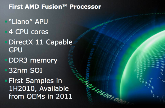
Late last year AMD said that before the end of 2010 it would be sampling its first APU (Accelerated Processing Unit) - codenamed Llano. Today AMD is announcing that the first Llano samples, built on Global Foundries 32nm high-k + metal gate, SOI process will be sampling to partners in the first half of this year.
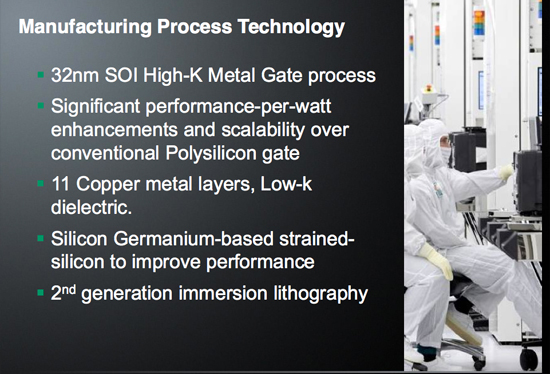
GF's 32nm SOI High-K + MG process will be used with Llano
For those not in the know, Llano is AMD’s first hybrid CPU-GPU with on-die graphics. The graphics core is a derivative of AMD’s DirectX 11 Evergreen lineup (the same lineage as the Radeon HD 5970, 5870, 5850, 5670, 5570, 5450, etc...).
Llano will go up against Sandy Bridge, which seems to have been pushed back to 2011 for volume availability according to Intel’s internal roadmaps. While Sandy Bridge will have graphics on-die, it will still only be DX10 class - AMD will have the feature-set advantage as far as graphics is concerned.

Llano's Features
Today we learn a bit more about the CPU side of Llano. The first chip will be a quad-core processor plus on-die graphics. Each core is Phenom II derived, but there’s no shared L3 cache. So Llano cores look a lot like Athlon II cores. I’m hearing that they may have some architectural tweaks, so performance could be better than present-day Athlon IIs.
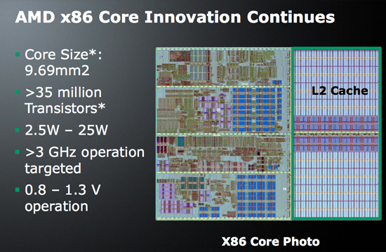
At 32nm each core (minus L2 cache) is only 9.69 mm^2 and is made up of over 35M transistors. Each core is paired with its own 1MB L2 cache, meaning the quad-core processor will have a total of 4MB of L2 on-die. AMD expects Llano to run at above 3GHz, which should be more than possible at 32nm given that we’re already at close to 3GHz with the 45nm Athlon II X4.
AMD’s First Power Gated CPU
With Nehalem Intel introduced power gating, a technique that allows a core to be near-completely powered down minimizing leakage current when inactive. This not only reduces idle power but it also enables Intel to use extra TDP to turbo up active cores.
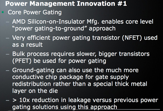
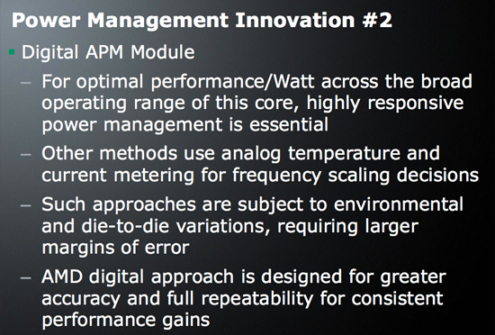
Llano uses power gating as well as a Digital APM Module. AMD doesn’t go into much detail on the digital APM module but I’m guessing we’ll see the same sort of turbo-like functionality out of Llano, including graphics turbo.
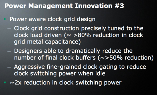
AMD also pointed out that Llano uses a “power aware clock grid design”. I couldn’t get much more information out of AMD on this one, other than its expecting a ~2x reduction in clock switching power. Simply distributing the clock to all parts of a modern day microprocessor can take up quite a bit of power, any improvements in efficiency there are very important.
I’ll keep digging to see if I can get any more details on this aspect of Llano.
Final Words
Llano will obviously require a new socket. All AMD is saying is that OEMs will be shipping systems in 2011. It’s unclear if we’ll see anything in the channel before then, but with sampling in the coming months it appears that AMD could be ready for Sandy Bridge when it arrives next year.
AMD isn’t qualifying its 2011 statement with an indication of what quarter to expect systems. Given that the first samples are going out now, I’d expect to see Llano sometime in the first half of 2011 but that’s purely conjecture on my part. Sandy Bridge is scheduled to ship in volume in the first quarter of 2011.
The big questions going forward are 1) how much AMD and Intel are going to scale up its graphics performance on these chips, and 2) how important DX11 support will be to the upcoming APU race.


58 Comments
View All Comments
stlbearboy - Monday, February 8, 2010 - link
They are not using DX11 for the graphics, they are the DirectCompute/Open CL functions. The hope is that software will be compiled using those API calls and thus will be faster on AMD silicon.MadMan007 - Monday, February 8, 2010 - link
If a program is compiled for a standardized API it won't favor one architecture over another due to the compiler, rather the architecture that is a better implementation will run the code faster.Tanclearas - Tuesday, February 9, 2010 - link
... so the "architecture" that has DX11 hardware (the "AMD silicon") would presumably be faster (or "favored") if a program is compiled with the standardized DC/OCL API.That's pretty much what was said, so I'm not sure what you were getting at in your reply.
stlbearboy - Monday, February 8, 2010 - link
DX11 has more compute features than DX10. So if a program is compiled in OpenCL, it will be able to perform more functions using the IGP on the AMD system than the Intel system. Kind of a reverse of optimizations on the CPU in which Intel normally included the instructions first.Alexvrb - Monday, February 8, 2010 - link
Bingo. DirectCompute 5.0 requires a DirectX 11 chip. With DX10 you get DC 4.0, with DX10.1 you get DC 4.1. Both are largely inferior to DC 5.0.Hiravaxis - Tuesday, February 9, 2010 - link
Will DC 5.0 go anywhere without Intel backing it?Or will this tech overlap at all with Nvidia's efforts with Fermi?
Alexvrb - Tuesday, February 9, 2010 - link
As Mr Perfect points out, DC 5.0 runs on any DX11 card. I'm sure it will run on future DX12 cards too. Even integrated DX11 solutions from Nvidia/AMD will be able to run DC 5.0 code, and thus accelerate a lot of parallel code. Not to mention that a piece of software can be written with both DC 4.0 and DC 5.0 code, much like having multiple rendering paths in 3D games.Mr Perfect - Tuesday, February 9, 2010 - link
AMD/ATI, Nvidia and Microsoft have all signed onto DX11 (which contains DirectCompute 5), so it's not waiting on Intel.