NVIDIA’s GeForce GTX 480 and GTX 470: 6 Months Late, Was It Worth the Wait?
by Ryan Smith on March 26, 2010 7:00 PM EST- Posted in
- GPUs
The GF100 Recap
NVIDIA first unveiled its GF100 (then called Fermi) architecture last September. If you've read our Fermi and GF100 architecture articles, you can skip this part. Otherwise, here's a quick refresher on how this clock ticks.
First, let’s refresh the basics. NVIDIA’s GeForce GTX 480 and 470 are based on the GF100 chip, the gaming version of what was originally introduced last September as Fermi. GF100 goes into GeForces and Fermi goes into Tesla cards. But fundamentally the two chips are the same.
At a high level, GF100 just looks like a bigger GT200, however a lot has changed. It starts at the front end. Prior to GF100 NVIDIA had a large unified front end that handled all thread scheduling for the chip, setup, rasterization and z-culling. Here’s the diagram we made for GT200 showing that:
NVIDIA's GT200
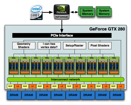
The grey boxes up top were shared by all of the compute clusters in the chip below. In GF100, the majority of that unified front end is chopped up and moved further down the pipeline. With the exception of the thread scheduling engine, everything else decreases in size, increases in quantity and moves down closer to the execution hardware. It makes sense. The larger these chips get, the harder it is to have big unified blocks feeding everything.
In the old days NVIDIA took a bunch of cores, gave them a cache, some shared memory and a couple of special function units and called the whole construct a Streaming Multiprocessor (SM). The GT200 took three of these SMs, added texture units and an L1 texture cache (as well as some scheduling hardware) and called it a Texture/Processor Cluster. The old GeForce GTX 280 had 10 of these TPCs and that’s what made up the execution engine of the GPU.
NVIDIA's GF100

Click to Enlarge
With GF100, the TPC is gone. It’s now a Graphics Processing Cluster (GPC) and is made up of much larger SMs. Each SM now has 32 cores and there are four SMs per GPC. Each GPC gets its own raster engine, instead of the entire chip sharing a larger front end. There are four GPCs on a GF100 (however no GF100 shipping today has all SMs enabled in order to improve yield).

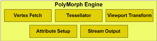
Each SM also has what NVIDIA is calling a PolyMorph engine. This engine is responsible for all geometry execution and hardware tessellation, something NVIDIA expects to be well used in DX11 and future games. NV30 (GeForce FX 5800) and GT200 (GeForce GTX 280), the geometry performance of NVIDIA’s hardware only increases roughly 3x in performance. Meanwhile the shader performance of their cards increased by over 150x. Compared just to GT200, GF100 has 8x the geometry performance of GT200, and NVIDIA tells us this is something they have measured in their labs. This is where NVIDIA hopes to have the advantage over AMD, assuming game developers do scale up geometry and tessellation use as much as NVIDIA is counting on.
NVIDIA also clocks the chip much differently than before. In the GT200 days we had a core clock, a shader clock and a memory clock. The core clock is almost completely out of the picture now. Only the ROPs and L2 cache operate on a separate clock domain. Everything else runs at a derivative of the shader clock. The execution hardware runs at the full shader clock speed, while the texture units, PolyMorph and Raster engines all run at 1/2 shader clock speed.
Cores and Memory
While we’re looking at GF100 today through gaming colored glasses, NVIDIA is also trying to build an army of GPU compute cards. In serving that master, the GF100’s architecture also differs tremendously from its predecessors.
All of the processing done at the core level is now to IEEE spec. That’s IEEE-754 2008 for floating point math (same as RV870/5870) and full 32-bit for integers. In the past 32-bit integer multiplies had to be emulated, the hardware could only do 24-bit integer muls. That silliness is now gone. Fused Multiply Add is also included. The goal was to avoid doing any cheesy tricks to implement math. Everything should be industry standards compliant and give you the results that you’d expect. Double precision floating point (FP64) performance is improved tremendously. Peak 64-bit FP execution rate is now 1/2 of 32-bit FP, it used to be 1/8 (AMD's is 1/5).

GT200 SM
In addition to the cores, each SM has a Special Function Unit (SFU) used for transcendental math and interpolation. In GT200 this SFU had two pipelines, in GF100 it has four. While NVIDIA increased general math horsepower by 4x per SM, SFU resources only doubled. The infamous missing MUL has been pulled out of the SFU, we shouldn’t have to quote peak single and dual-issue arithmetic rates any longer for NVIDIA GPUs.

GF100 SM
NVIDIA’s GT200 had a 16KB shared memory in each SM. This didn’t function as a cache, it was software managed memory. GF100 increases the size to 64KB but it can operate as a real L1 cache now. In order to maintain compatibility with CUDA applications written for G80/GT200 the 64KB can be configured as 16/48 or 48/16 shared memory/L1 cache. GT200 did have a 12KB L1 texture cache but that was mostly useless for CUDA applications. That cache still remains intact for graphics operations. All four GPCs share a large 768KB L2 cache.

Each SM has four texture units, each capable of 1 texture address and 4 texture sample ops. We have more texture sampling units but fewer texture addressing units in GF100 vs. GT200. All texture hardware runs at 1/2 shader clock and not core clock.
| NVIDIA Architecture Comparison | G80 | G92 | GT200 | GF100 | GF100 Full* |
| Streaming Processors per TPC/GPC | 16 | 16 | 24 | 128 | 128 |
| Texture Address Units per TPC/GPC | 4 | 8 | 8 | 16 | 16 |
| Texture Filtering Units per TPC/GPC | 8 | 8 | 8 | 64 | 64 |
| Total SPs | 128 | 128 | 240 | 480 | 512 |
| Total Texture Address Units | 32 | 64 | 80 | 60 | 64 |
| Total Texture Filtering Units | 64 | 64 | 80 | 240 | 256 |
Last but not least, this brings us to the ROPs. The ROPs have been reorganized, there are now 48 of them in 6 parttions of 8, and a 64bit memory channel serving each partition. The ROPs now share the L2 cache with the rest of GF100, while under GT200 they had their own L2 cache. Each ROP can do 1 regular 32bit pixel per clock, 1 FP16 pixel over 2 clocks, or 1 FP32 pixel over 4 clocks, giving the GF100 the ability to retire 48 regular pixels per clock. The ROPs are clocked together with the L2 cache.
Threads and Scheduling
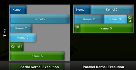
While NVIDIA’s G80 didn’t start out as a compute chip, GF100/Fermi were clearly built with general purpose compute in mind from the start. Previous architectures required that all SMs in the chip worked on the same kernel (function/program/loop) at the same time. If the kernel wasn’t wide enough to occupy all execution hardware, that hardware went idle, and efficiency dropped as a result. Remember these chips are only powerful when they’re operating near 100% utilization.
In this generation the scheduler can execute threads from multiple kernels in parallel, which allowed NVIDIA to scale the number of cores in the chip without decreasing efficiency.
GT200 (left) vs. GF100 (right)
With a more compute leaning focus, GF100 also improves switch time between GPU and CUDA mode by a factor of 10x. It’s now fast enough to switch back and forth between modes multiple times within a single frame, which should allow for more elaborate GPU accelerated physics.
NVIDIA’s GT200 was a thread monster. The chip supported over 30,000 threads in flight. With GF100, NVIDIA scaled that number down to roughly 24K as it found that the chips weren’t thread bound but rather memory bound. In order to accommodate the larger shared memory per SM, max thread count went down.
| GF100 | GT200 | G80 | |
| Max Threads in Flight | 24576 | 30720 | 12288 |
NVIDIA groups 32 threads into a unit called a warp (taken from the looming term warp, referring to a group of parallel threads). In GT200 and G80, half of a warp was issued to an SM every clock cycle. In other words, it takes two clocks to issue a full 32 threads to a single SM.
In previous architectures, the SM dispatch logic was closely coupled to the execution hardware. If you sent threads to the SFU, the entire SM couldn't issue new instructions until those instructions were done executing. If the only execution units in use were in your SFUs, the vast majority of your SM in GT200/G80 went unused. That's terrible for efficiency.
Fermi fixes this. There are two independent dispatch units at the front end of each SM in Fermi. These units are completely decoupled from the rest of the SM. Each dispatch unit can select and issue half of a warp every clock cycle. The threads can be from different warps in order to optimize the chance of finding independent operations.
There's a full crossbar between the dispatch units and the execution hardware in the SM. Each unit can dispatch threads to any group of units within the SM (with some limitations).
The inflexibility of NVIDIA's threading architecture is that every thread in the warp must be executing the same instruction at the same time. If they are, then you get full utilization of your resources. If they aren't, then some units go idle.
A single SM can execute:
| GF100 | FP32 | FP64 | INT | SFU | LD/ST |
| Ops per clock | 32 | 16 | 32 | 4 | 16 |
If you're executing FP64 instructions the entire SM can only run at 16 ops per clock. You can't dual issue FP64 and SFU operations.
The good news is that the SFU doesn't tie up the entire SM anymore. One dispatch unit can send 16 threads to the array of cores, while another can send 16 threads to the SFU. After two clocks, the dispatchers are free to send another pair of half-warps out again. As I mentioned before, in GT200/G80 the entire SM was tied up for a full 8 cycles after an SFU issue.
The flexibility is nice, or rather, the inflexibility of GT200/G80 was horrible for efficiency and Fermi fixes that.


196 Comments
View All Comments
ol1bit - Thursday, April 1, 2010 - link
I thought it was a fare review. They talked about the heat issues, etc.You can't compare a 2 GPU card to a single GPU card. If they ever make a 2 core GF100, I'm sure Anandtech will do a review.
IceDread - Tuesday, April 6, 2010 - link
You are wrong. You can and you should compare single gpu cards with multi gpu cards. It does not matter if a card has one or 30 gpu's on the card. It's the performance / price that matters.These nvidia cards are very expensive in performance / price compared to the ATI cards, simple as that. It's obvious that nvidia dropped the ball with their new flagship. You even need 2 cards to be able to use 3 screens.
This is bad for us customers, we are not getting any price pressure at all. These nvidia cards does not improve the market since they can not compete with the ATI card, only nvidia fans will purchase these cards or possibly some working with graphics.
I hope nvidia will do better with their next series or cards and I hope that won't take to long because ATI will most likely release a new series in half a year or so.
xxtypersxx - Sunday, March 28, 2010 - link
I will be interested in seeing the performance gains that will likely come from revised Nvidia drivers in a month or two. In some of the tests the gtx470 is trading blows with the gtx285 despite having nearly double the compute power...I think there is a lot of room for optimization.I am no fanboy and even owned a 4850 for a while, but Nvidia's drivers have always been a big decision factor for me. I don't get any of the random issues that were common on catalyst and aside from the occasional hiccup (196.67 G92 fan bug) I don't worry about upgrades breaking things. I admit I don't know if all the 5xxx series driver issues have been fixed yet but I do look forward to driver parity, until then I think raw performance is only part of the equation.
GourdFreeMan - Sunday, March 28, 2010 - link
Ryan, have you checked performance and/or clocks to see if any of the cards you are testing are throttling under FurMark? I recall you mentioning in your 58xx review that ATi cards can throttle under FurMark to prevent damage, and while most of the power numbers look normal, I notice a few of the cards are consuming less power under FurMark than Crysis, unlike the majority of the cards which consume considerably more power running FurMark than Crysis...MojaMonkey - Sunday, March 28, 2010 - link
I can turn off one light in my house and remove the power consumption difference between the GTX480 and the 5870.I thought this was an enthusiast site?
I lol irl when people talk about saving 100 watts and buying a 5870. So saving 100 watts but building a 700 watt system? Are you saving the planet or something?
I think nVidia is smart, if you fold or use cuda or need real time 3d performance from a quadro you will buy this card. That probably is a large enough market for a niche high end product like this.
PS: 5870 is the best gaming card for the money!
Paladin1211 - Sunday, March 28, 2010 - link
No, the 5850 is.p/s: I misclicked the Report instead of Reply button, so pls ignore it T_T
kallogan - Sunday, March 28, 2010 - link
Seriously i wonder who'd want gpus that power angry, noisy and hot...Nvidia is out both on mobile and desktop market...The only pro for Nvidia i can see is the 3D support.beginner99 - Sunday, March 28, 2010 - link
This is kind of bad for consumers. 0 pressure on ATI to do anything from lower price to anything else. they can just lay back and work on the next gen.Well, that at least made my decision easy. build now or wait for sandybridge. I will wait. hoepfully gpu marekt will be nicer then too (hard to be worse actually).
C5Rftw - Sunday, March 28, 2010 - link
I was waiting for the fermi cards to come out before my next high end build( looking for price drops), but I actually did not expect this card to be this fast. The GTX480 is ~15% faster than the 5870, but for $100 more, and it is just gonna be a Nvidia loyal card, and the 5870 will probably drop just a little if at all.. The 5850 and and 5830 should drop $25-50, hopefully more(2x5850 at ~250$ each would be FTW). Now, would I like to have a fermi?, well yeah for sure, but I would much rather have a 5870 and down the road add another. A GTX 480 uses the same, if not more power than (2) 5870's. Now this reminds me of the last gen of the P4's. or as we know em, the Preshots. Basically, Nvidia's idea of a huge chip approach, with yes impressive performance, was just the wrong approach. I mean, their next-gen, if based on this same "doubling" SPs, cuda cores, would draw 300w+ easily and almost require water cooling because the next TSMC process is going to be 32nm and that will not allow them to "cut the chip in half." ATI's theory started with the 4000 series has proven to be a much better/efficient design. I think they could make a 6870 using 40nm TSMC right now, but ofcourse it would be a hot chip. Now when they get the 32 TSMC FABs running, Nvidia has got to re-design their chips.. And with how hot the GTX 480 is, I dont see how they could make a GTX 495. Also, the 5890 is right around the corner and that should give the final punch to KO Nvidia in this GPU generation. On a side note, Thank " " that there is some healthy competion or AMD might pull what Nvidia did and rebrand the 8800 5 or 6 times.Belard - Sunday, March 28, 2010 - link
Keep in mind, the GeForce 480 (GTX means nothing, see any GTX210 or GT 285?) is already the most power hungry card on the market, just under 300watts under full load.... if the GF480 had all 512 Cuda Cores running and clocked higher... the card will easily surpass 300watts!This in turn means MORE heat, more power, more noise. There are videos on the 480/470s & ATI cards... the 480's fan is running very fast and loud to keep it under 100c, about 2~3 times hotter than a typical CPU.
We will see the ATI 6000 series on 40nm, but it may not be with TSMC.
If the upcoming 5890 is 15% faster and can sell for $400~450, that would put some hurt on the GF480.
Not sure how/why ATI would do re-branding. The 4670 is almost like a 3870, but is easily a more advanced and cheaper GPU. The bottom end GPUs have all changed. 2400 / 3450, 4350, 5450 - all different.
Nvidia has been doing re-branding for quite a long time. The GF2mx was re-branded as the GF2MX 400 (These were bottom end $150~190 cards in 2001) and then for some bone-head reason, during the GF6 era - they brought back the GF2MX but added DX8. Huh? Add a function to an OLD bottom end GPU?
The GF2-TI came out when GF3-TI series was launched... they wanted "TI" branding. The GF2-TI was a rebranded GF2-Pro with a slight clock upgrade.
Then came the first big-branding/feature fiasco with Nvidia. The GF8 was the first DX8 cards. Then the GF 4 series came out. The GF4ti were the high end models. But the MX series were nothing more than GF2 (DX7) with optional DVI... to take care of the low end and shove the letter names to the front.
GF4 mx420 = GF2mx, but a bit slower.
GF4 mx440 = GF2 Pro/TI
GF4 mx460 = ... faster DX7 card, but it was about $20~35 cheaper than the GF4-TI4200, a DX8 card. The Ti4200 was a #1 seller at about $200. Some of the 440se & 8x models may have 64 or 128bit RAM... ugh.
Then they had fun with the TI series when AGP 8x came out... NEW models! Either thou the cards couldn't max out the AGP 4x bus. Even the future ATI 9800Pro only ran 1~3% faster with AGP 8x.
GF4 Ti 4200 > GF4 Ti 4200 8x
GF4 Ti 4400 > GF4 Ti 4800 SE
GF4 Ti 4600 > GF4 Ti 4800
Yep, same GPUs... new names. Some people would upgrade to nothing or worse. Some even went from the 4600 to the 4800SE which was a downgrade!
GF5 5500 = 5200
Since the GF5... er "FX" series, Nvidia kept the DX# and feature set within the series. All GF5 cards are DX9.
But the 5200s were a joke. By the time they hit the market at $120, the Ti4200s were also $120 and the 4mx were reduced to $30~60. But the 5200 was HALF the performance of a 4200. People actually thought they were upgrading... returns happened.
Funny thing once. A person bought a "5200" at walmart and was confused by the POST display of "4200". Luckily he had posted to us on the interent. We laughed our butts off...! What happened? Batch & switch... someone bought a 5200, took it home - switched cards, took it back to Walmart for a refund. hey, its usually a brick or a dead card, etc. he got used card, but a much better product.
Like the ATI 5450 is too slow for gaming today for DX11, the GF5200 was horrible back in 2003 for DX9! The 5200 is still sold today, the only thing left.
Pretty much the entire GF5 series was utter garbage. 4 versions of the GF5600 ($150~200) were slower than the previous $100 Ti 4200. It was sick. This allowed ATI to gain respect and marketshare with their ATI 9600 & 9700 cards. The GF 5700 series (2 out of 5 types) were good Ti4200 replacements. The 5900 went up against the ATI 9800. I've owned both.
Since then, ATI pretty much had the upper hand in performance throughout the GF6 & GF7 era. AMD buys out ATI, then the GF8 and core2 wipes out ATI/AMD with faster products.
While ATI had the faster cards during DX9.0c (really MS? Couldn't make 6.1, 6.2?) era over the GF6/7... Nvidia *HAD* the lower end market. The GF6600 and 7600GT were $150~200 products... ATI products in that price range were either too slow or cost too much.
With GF 8800 & 8600s, ATI had lost high & mid-range markets. The HD 2000 series = too expensive, too hot and not fast enough... (sound familiar). The ATI 3000 series brought ATI back to competitive position where it counted. Meanwhile, Nvidia milked the G92~96 for the past 2+ years. They are code-name & model number crazy happy.
As long as ATI continues doing engineering and management this way, nVidia will continue to be in trouble for a long time unless they get their act together or count on the server market to stay in business.
End of short history lesson :0