NVIDIA’s GeForce GTX 480 and GTX 470: 6 Months Late, Was It Worth the Wait?
by Ryan Smith on March 26, 2010 7:00 PM EST- Posted in
- GPUs
Prologue
Because designing GPUs this big is "[redacted] hard"
-NVIDIA’s VP of Product Marketing Ujesh Desai on GF100
Fermi/GF100/GTX400 has been a long time coming. For an industry where the major players are usually in lockstep with each other in some fashion, this latest cycle has been distinctly out of sync. In September of 2009 we saw AMD launch their Radeon 5000 series, and spend the next 6 months as the performance leader for the discrete graphics market for virtually every price point. NVIDIA on the other hand missed the latest cycle by a mile, and when AMD was delivering 5000 series cards NVIDIA could only talk about the High Performance Computing applications of their next GPU, Fermi. It would be the next big thing, both figuratively and literally.
In January we got the next piece of the Fermi story at CES, when NVIDIA was willing to talk about the gaming-oriented hardware and applications of the first Fermi GPU: GF100. We found out it would be significantly different from the GT200 GPU powering NVIDIA’s GTX200 series, that NVIDIA was going to break up the traditional fixed-function pipeline and at the same time take a particularly keen interest in tessellation. What we didn’t find out is when it would ship.
Much of this has been in NVIDIA’s hands – some of it has not. What’s indisputable is that TSMC, the chip foundry used by both AMD and NVIDIA, was not delivering the kind of yields on their 40nm process that AMD and NVIDIA were expecting. Both of them suffered for it. AMD could not get enough viable chips to meet demand for their 5000 series part, leaving a wake of disappointed gamers who could not get AMD’s latest wonder, and limiting AMD’s ability to profit from one of the few times in AMD/ATI’s history where the company had a clear lead over NVIDIA, and if you ask AMD also limiting their ability to control prices. NVIDIA meanwhile had to deal with the fact that they were trying to produce a very large chip on a low-yielding process, a combination for disaster given that size is the enemy of high yields.
What’s also indisputable is that this 6 month wait has benefited few people. For the observers of an industry where the competition is cut-throat we saw GPU prices rise, when in the last generation AMD and NVIDIA knocked upwards of hundreds of dollars off of each other’s prices practically overnight. It may have been good times overall for AMD, but for buyers the competitive marketplace is sorely missed.
That brings us to today. We can see the light at the end of the tunnel, the end of NVIDIA’s 6 month journey is near. We’ve told you about the compute applications of Fermi, we’ve told you about the gaming applications of Fermi, and now at long last we can tell you about the first products. It’s time to say hello to the GTX 400 series.
Meet the GTX 480 and GTX 470
| GTX 480 | GTX 470 | GTX 295 | GTX 285 | 9800+ GTX | |
| Stream Processors | 480 | 448 | 2 x 240 | 240 | 128 |
| Texture Address / Filtering | 60/60 | 56/56 | 2 x 80 / 80 | 80 / 80 | 64 / 64 |
| ROPs | 48 | 40 | 2x 28 | 32 | 16 |
| Core Clock | 700MHz | 607MHz | 576MHz | 648MHz | 738MHz |
| Shader Clock | 1401MHz | 1215MHz | 1242MHz | 1476MHz | 1836MHz |
| Memory Clock | 924MHz (3696MHz data rate) GDDR5 | 837MHz (3348MHz data rate) GDDR5 | 999MHz (1998MHz data rate) GDDR3 | 1242MHz (2484MHz data rate) GDDR3 | 1100MHz (2200MHz data rate) GDDR3 |
| Memory Bus Width | 384-bit | 320-bit | 2 x 448-bit | 512-bit | 256-bit |
| Frame Buffer | 1.5GB | 1.25GB | 2 x 896MB | 1GB | 512MB |
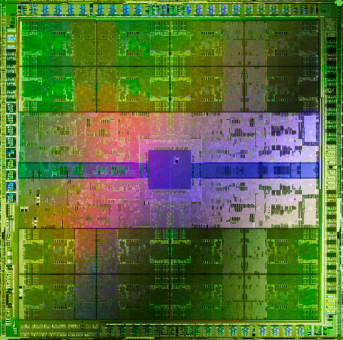
| Transistor Count | 3B | 3B | 2 x 1.4B | 1.4B | 754M |
| Manufacturing Process | TSMC 40nm | TSMC 40nm | TSMC 55nm | TSMC 55nm | TSMC 55nm |
| Price Point | $499 | $349 | $500 | $400 | $150 - 200 |
Today NVIDIA is launching two cards: the GeForce GTX 480, and the GeForce GTX 470. Both of them are based on GF100, the first and largest member of the Fermi family. Right off the bat, we can tell you that neither card is a complete GF100 chip. We know from NVIDIA’s earlier announcements that a complete GF100 is a 512 SP/core part organized in a 4x16x32 fashion, but these first parts will not have all of GF100’s functional units activated. Instead we’ll be getting a 480 core part for the GTX 480, and a 448 core part for the GTX 470. Ultimately we will not be seeing the full power of GF100 right away, but you can be sure that somewhere down the line we’ll see a GTX 485 or GTX 490 with all of GF100’s functional units enabled.
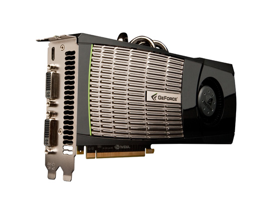
NVIDIA's GeForce GTX 480
What we’re starting out with today at the high-end is the GTX 480, a card based on a GF100 with 1 of the 16 SMs disabled that will sell for $499, making it the primary competitor for the Radeon 5870. The disabled SM has no affect on the ROPs which are part of a separate functional block, but it does cut down on the shading, texturing, and tessellation capabilities of the card compared to where a full GF100 card would be. This gives the GTX 480 the full 48 ROPs and 768KB of L2 cache of GF100, along with 60 texture units, 15 PolyMorph engines, and 480 cores. Although the architectural overhaul means we can’t compare the GTX 480 to the GTX 285 quite as easily as we could the Radeon 5000 series to the Radeon 4000 series, the GTX 480 is still in some ways a doubled-up GTX 285 from a shader standpoint.
The GTX 470 on the other hand is a further cut-down GF100-based product that will sell for $349. As we stated earlier it has only 448 cores, a product of NVIDIA disabling 2 of the 16 SMs. Along with disabling the SMs, NVIDIA also disabled 1 of the 6 ROP clusters, which disables 6 ROPs, 128KB of L2 cache, and 2 of the 32bit memory channels. This leaves us with 448 cores running alongside 40 ROPs, 640KB of L2 cache, all on a 320bit GDDR5 memory bus.
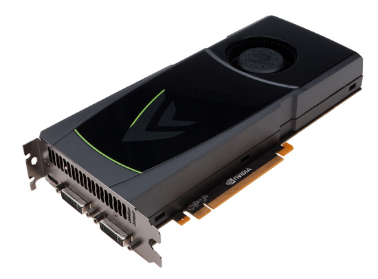
NVIDIA's GeForce GTX 470
As is usually the case for a harvested part, GTX 470 takes a clockspeed hit compared to GTX 480. The core clock falls 13% to 607MHz, and the shader clock falls the same distance to 1215MHz. The memory clock on the other hand only drops by 10% to 837MHz (3348MHz effective). Overall this gives the GTX 470 around 80% of the shading, texturing, and tessellation capabilities of the GTX 480 and 72% of the ROP capability and memory bandwidth.
One thing that caught our eye with all of this was that NVIDIA’s memory clocks are lower than we had been initially expecting. GDDR5 is readily available up to 5GHz while NVIDIA doesn’t go any higher than 3.7GHz; in fact between the smaller memory bus than the GTX 285 and the lower than expected memory clocks, the GTX 400 series doesn’t have all that much more bandwidth than the GTX 285 did. As it stands the GTX 480 only has 11% more memory bandwidth than the GTX 285, while the GTX 470 has 15% less than the GTX 285.
Given the 384-bit bus, we initially assumed NVIDIA was running in to even greater memory bus issues than AMD ran in to for the 5000 series, but as it turns out that’s not the case. When we asked NVIDIA about working with GDDR5, they told us that their biggest limitation wasn’t the bus like AMD but rather deficiencies in their own I/O controller, which in turn caused them to miss their targeted memory speeds. Unlike AMD who has been using GDDR5 for nearly 2 years, NVIDIA is still relatively new at using GDDR5 (their first product was the GT 240 late last year), so we can’t say we’re completely surprised here. If nothing else, this gives NVIDIA ample room to grow in the future if they can get a 384-bit memory bus up to the same speeds as AMD has gotten their 256-bit bus.
This leaves us with the other elephant in the room: yield on GF100. NVIDIA hasn’t commented specifically on the yields coming out of TSMC but we know even 6 months later that AMD still isn’t satisfied with things, so that should offer some guidance on the situation given NVIDIA’s larger die. As it stands NVIDIA chose to launch their highest end GF100 part with only 15 of 16 SMs in order to reach the “broadest availability”, which is a clear sign that NVIDIA isn’t getting enough full-yielding and high-clocking dies at this time to offer a proper unharvested part.
The power/heat situation also bears mentioning, since it often goes hand-in-hand with yield issues. With a 500mm2+ die on the 40nm process, it should come as no surprise that both the GTX 480 and GTX 470 are hot cards. NVIDIA has to pay the piper for having such a large die, and this is one of the places where they do so. The TDP for the GTX 480 is 250W while it’s 215W for the GTX 470; meanwhile the cards idle at 47W and 33W respectively. NVIDIA’s large die strategy usually leads to them having power-hungry parts, but from a historical perspective the GTX 480 is the hungriest yet for a single-GPU card; even the GTX280 wasn’t quite as high. We’ll get in to this more when we take a look at measured power consumption.


196 Comments
View All Comments
Ryan Smith - Saturday, March 27, 2010 - link
Yes, we did. We were running really close to the limits of our 850W Corsair unit. We measured the 480SLI at 900W, which after some power efficiency math comes out to around 750-800W actual load. At that load there's less extra space than we'd like to have.Just to add to that, we had originally been looking for a larger PSU after talking about PSU requirements with an NVNDIA partner, as the timing of this required we secure a new PSU before the cards arrived. So Antec had already shipped us their 1200W PSU before we could test the 850W, and we're glad since we would have been cutting it so close.
bigboxes - Sunday, March 28, 2010 - link
Appreciate the reply.GullLars - Saturday, March 27, 2010 - link
OK, so 480 generally beats 5870, and 470 generally beats 5850, but at higher prices, temperatures, wattage, and noise levels. What about 5970?As far as i can tell, the 5970 beat or came even with 480 in all tests, draws less power, runs cooler, and makes less noise. The price isn't that much more either.
It seems more fair to me to compare 480 with 5970 as both are the fastest single-card (as in PCIe slot) sollutions and are close in price and wattage.
I would also like to see what framerate FPS games come in at with gamer settings (1680x1050 and 1920x1200 resolutions), and if average is higher than game cutoff or tickrate, what is the minimum FPS, and how much can you bump eyecandy before avg drops below cutoff/tickrate or minimum drops below acceptable (30).
The reason for gamers sacraficing visuals to get high FPS can be summarized to game flow and latency. If FPS is below game tickrate, you get latency. For many games the tickrate is around 100 (100 updates in the game engine pr second). At 100 FPS you have 10ms latency between frames, if it drops to 50 you have 20 ms, and at 25 you have 40 ms. Lower than 25-30 FPS will obviously also result in virtually unplayable performance since aiming will becoming hard, so added latency from FPS below this becomes moot. If you are playing multiplayer games, this is added to the network latency. As most gamers know, latency below 30ms is generally desired, and above 50ms starts to matter, and above 100ms is very noticable. If you are on a bad connection (or have a bad connection to the server), 20-30ms added latency starts to matter even if it isn't visually notable.
bigboxes - Saturday, March 27, 2010 - link
Anyone else getting that message? I finally had to turn off the 'attack site' option in FF. It wasn't doing this last night. It's not doing it all over AT, just on the GTX 480 article.GullLars - Saturday, March 27, 2010 - link
Here too, it listed among others googleanalytics.com as a hostile site.It was probebly because NVidia wasn't happy with the review XD
(just joking ofc)
chrisinedmonton - Saturday, March 27, 2010 - link
Great article. Here's a small suggestion; temperature graphs should be normalised to room temperature rather than to 0C.GourdFreeMan - Sunday, March 28, 2010 - link
I agree. Temperature graphs should either be normalized to the ambient environment or absolute zero; any other choice of basis is completely arbitrary.Ahmed0 - Saturday, March 27, 2010 - link
Uh oh, my browser just got a heartwarming warning when I clicked on this article, the warning said that it might infect my computer badly and that I should definitely run home faster than my legs can carry.So, whats up with that?
Lifted - Saturday, March 27, 2010 - link
I just got that too. Had to disable the feature in Firefox.NJoy - Saturday, March 27, 2010 - link
well, Charlie was semi-accurate, but quite right =))What a hot chick... I mean, literately hot. Way too hot