NVIDIA's GeForce GTX 580: Fermi Refined
by Ryan Smith on November 9, 2010 9:00 AM ESTThe GTX 480… it’s hotter, it’s noisier, and it’s more power hungry, all for 10-15% more performance. If you need the fastest thing you can get then the choice is clear, otherwise you’ll have some thinking to decide what you want and what you’re willing to live with in return.
The GeForce GTX 480 and the associated GF100 GPU have presented us with an interesting situation over the last year. On the one hand NVIDIA reclaimed their crown for the fastest single GPU card on the market, and in time used the same GPU to give rise to a new breed of HPC cards that have significantly expanded the capabilities of GPU computing. On the other hand, like a worn and weary athlete finally crossing the finish line, this didn’t come easy for NVIDIA. GF100 was late, and the GTX 480 while fast was still hot & loud for what it was.
Furthermore GTX 480 and GF100 were clearly not the products that NVIDIA first envisioned. We never saw a product using GF100 ship with all of its SMs enabled – the consumer space topped out at 15 of 16 SMs, and in the HPC space Tesla was only available with 14 of 16 SMs. Meanwhile GF100’s younger, punchier siblings put up quite a fight in the consumer space, and while they never were a threat to GF100, it ended up being quite the surprise for how close they came.
Ultimately the Fermi architecture at the heart of this generation is solid – NVIDIA had to make some tradeoffs to get a good gaming GPU and a good compute GPU in a single product, but it worked out. The same can’t be said for GF100, as its large size coupled with TSMC’s still-maturing 40nm process lead to an unwieldy combination that produced flakey yields and leaky transistors. Regardless of who’s ultimately to blame, GF100 was not the chip it was meant to be.
But time heals all wounds. With GF100 out the door NVIDIA has had a chance to examine their design, and TSMC the chance to work the last kinks out of their 40nm process. GF100 was the first Fermi chip, and it would not be the last. With a lesson in hand and a plan in mind, NVIDIA went back to the drawing board to fix and enhance GF100. The end result: GF110, the next iteration of Fermi. Hot out of the oven, it is launching first in the consumer space and is forming the backbone of the first card in NVIDIA’s next GeForce series: GeForce 500. Launching today is the first such card, the GF110-powered GeForce GTX 580.
| GTX 580 | GTX 480 | GTX 460 1GB | GTX 285 | |
| Stream Processors | 512 | 480 | 336 | 240 |
| Texture Address / Filtering | 64/64 | 60/60 | 56/56 | 80 / 80 |
| ROPs | 48 | 48 | 32 | 32 |
| Core Clock | 772MHz | 700MHz | 675MHz | 648MHz |
| Shader Clock | 1544MHz | 1401MHz | 1350MHz | 1476MHz |
| Memory Clock | 1002MHz (4008MHz data rate) GDDR5 | 924MHz (3696MHz data rate) GDDR5 | 900Mhz (3.6GHz data rate) GDDR5 | 1242MHz (2484MHz data rate) GDDR3 |
| Memory Bus Width | 384-bit | 384-bit | 256-bit | 512-bit |
| Frame Buffer | 1.5GB | 1.5GB | 1GB | 1GB |
| FP64 | 1/8 FP32 | 1/8 FP32 | 1/12 FP32 | 1/12 FP32 |
| Transistor Count | 3B | 3B | 1.95B | 1.4B |
| Manufacturing Process | TSMC 40nm | TSMC 40nm | TSMC 40nm | TSMC 55nm |
| Price Point | $499 | ~$420 | ~$190 | N/A |
GF110 is a mix of old and new. To call it a brand-new design would be disingenuous, but to call it a fixed GF100 would be equally shortsighted. GF110 does have a lot in common with GF100, but as we’ll see when we get in to the design of GF110 it is its own GPU. In terms of physical attributes it’s very close to GF100; the transistor count remains at 3 billion (with NVIDIA undoubtedly taking advantage of the low precision of that number), while the die size is at 520mm2. NVIDIA never did give us the die size for GF100, but commonly accepted values put it at around 530mm2, meaning GF110 is a hair smaller.
But before we get too deep in to GF110, let’s start with today’s launch card, the GeForce GTX 580. GTX 580 is the first member of the GeForce 500 series, giving it the distinction of setting precedent for the rest of the family that NVIDIA claims will soon follow. Much like AMD last month, NVIDIA is on their second trip with the 40nm process, meaning they’ve had the chance to refine their techniques but not the opportunity to significantly overhaul their designs. As a result the 500 series is going to be very familiar to the 400 series – there really aren’t any surprises or miracle features to talk about. So in many senses, what we’re looking at today is a faster version of the GTX 480.
So what makes GTX 580 faster? We’ll start with the obvious: it’s a complete chip. All the L2 cache, all the ROPs, all the SMs, it’s all enabled. When it comes to gaming this is as fast as GF110 can be, and it’s only through NVIDIA’s artificial FP64 limitations that double-precision computing isn’t equally unrestricted. We have wondered for quite some time what a full GF100 chip would perform like – given that GTX 480 was short on texture units, shaders, and polymorph engines, but not ROPs – and now the answer is at hand. From all of this GTX 580 has 6.6% more shading, texturing, and geometric performance than the GTX 480 at the same clockspeeds. Meanwhile the ROP count and L2 cache remains unchanged; 48 ROPs are attached to 768KB L2 cache, which in turn are attached to 6 64bit memory controllers.
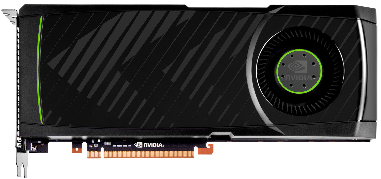
GeForce GTX 580
The second change of course is clockspeeds. The reference GTX 480 design ran at 700MHz for the core and 924MHz (3696MHz data rate) for the GDDR5. Meanwhile GTX 580 brings that up to 772MHz for the core and 1002MHz (4008MHz data rate), marking a 72MHz(10%) increase in core clockspeed and a slightly more modest 78MHz (8%) increase in memory bandwidth. This is a near-equal increase in the amount of work that GTX 580 can process and the amount of work its memory can feed it, which should offer a relatively straightforward increase in performance.
Last but certainly not least change coming from GTX 480 is in GF110 itself. NViDIA has ported over GF104’s faster FP16 (half-precision) texture filtering capabilities, giving GF110/GTX580 the ability to filter 4 FP16 pixels per clock, versus 2 on GF100/GTX480. The other change ties in well with the company’s heavy focus on tessellation, with a revised Z-culling/rejection engine that will do a better job of throwing out pixels early, giving GF110/GTX580 more time to spend on rendering the pixels that will actually be seen. This is harder to quantify (and impossible for us to test), but NVIDIA puts this at another 8% performance improvement.
Meanwhile NVIDIA hasn’t ignored GTX 480’s hot and loud history, and has spent some time working on things from that angle. We’ll dive in to NVIDIA’s specific changes later, but the end result is that through some optimization work they’ve managed to reduce their official TDP from 250W on the GTX 480 to 244W on the GTX 580, and in practice the difference is greater than that. NVIDIA’s cooling system of choice has also been updated, working in tandem with GTX 580’s lower power consumption to bring down temperatures and noises. The end result is a card that should be and is cooler and quieter while at the same being faster than GTX 480.
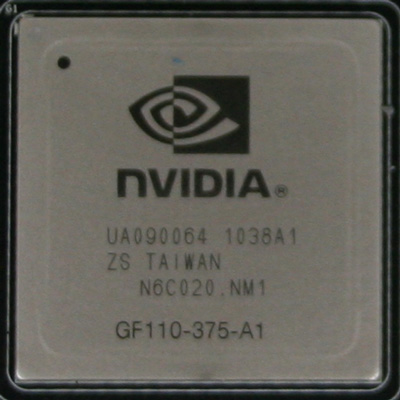
GF110
The downside to this is that if it sounds like a fairy tale, it almost is. As you’ll see we have a rather high opinion of GTX 580, but we’re not convinced you’re going to be able to get one quite yet. NVIDIA is technically hard-launching GTX 580 today at $499 (GTX 480’s old price point), but they aren’t being very talkative about the launch quantity. They claim it’s for competitive reasons (to keep AMD from finding out) and we can certainly respect that, but at the same time it’s rare in this industry for someone to withhold information because it’s a good thing. We really hope to be surprised today and see GTX 580s available for everyone that wants one, but we strongly suspect that it’s going to be available in low quantities and will sell out very quickly. After that it’s anyone’s guess on what the refresh supply will be like; our impression of matters is that yields are reasonable for such a large chip, but that NVIDIA didn’t spend a lot of time stockpiling for today’s launch.
In any case, with GTX 580 taking the $500 spot and GF110 ultimately destined to replace GF100, GF100 based cards are going to be on their way out. NVIDIA doesn’t have an official timeline, but we can’t imagine they’ll continue producing GF100 GPUs any longer than necessary. As a result the GTX 480 and GTX 470 are priced to go, falling between the GTX 580 and the GTX 460 in NVIDIA’s lineup for now until they’re ultimately replaced with other 500 series parts. For the time being this puts the GTX 480 at around $400-$420, and the GTX 470 – still doing battle with the Radeon HD 6870 – is at $239-$259.
Meanwhile AMD does not have a direct competitor for the GTX 580 at the moment, so their closest competition is going to be multi-GPU configurations. In the single card space there’s the Radeon HD 5970, which is destined for replacement soon and as a result AMD is doing what they can to sell off Cypress GPUs by the end of the year. The last reference 5970 you can find on Newegg is a Sapphire card, which is quite blatantly priced against the GTX 580 at $499 with a $30 rebate. Given that it’s the last 5970, we’d be surprised if it was in stock for much longer than the initial GTX 580 shipments.
For cards you do stand a good chance of getting, a pair of 6870s will set you back between $480 and $500, making it a straightforward competitor to the GTX 580 in terms of price. A pair of cards isn’t the best competitor, but CrossFire support is widely available on motherboards so it’s a practical solution at that price.
| Fall 2010 Video Card MSRPs | ||
| NVIDIA | Price | AMD |
|
GeForce GTX 580
|
$500 | Radeon HD 5970 |
| $420 | ||
|
|
$300 | Radeon HD 5870 |
| $240 | Radeon HD 6870 | |
| $180 | Radeon HD 6850 | |


160 Comments
View All Comments
knutjb - Tuesday, November 9, 2010 - link
I agree guys it should be a 485 not a 580.The 6870 is a sore spot on an otherwise solid refinement. Curious to see its SLI performance. $559 on Newegg this am.
dtham - Tuesday, November 9, 2010 - link
Anyone know if aftermarket cooling for the GTX 480 will work for the GTX 580? It would be great to be able to reuse a waterblock from a GTX 480 for the new 580s. Looking at the picture the layout looks similar.mac2j - Tuesday, November 9, 2010 - link
In Europe the GTX 580 was launched at 399 Euros and in response ATI has lowered the 5970 to 389 Euros (if you believe the rumors).This can only bode well for holiday prices of the 6970 vs 580.
samspqr - Tuesday, November 9, 2010 - link
it's already listed and in stock at alternate.de, but the cheapest one is 480eurthe only 5970 still in stock there is 540eur
yzkbug - Tuesday, November 9, 2010 - link
I moved all my gaming to the living room on a big screen TV and HTPC (a next next gen console in a sense). But, Optimus would be the only way to use this card on HTPC.slatr - Tuesday, November 9, 2010 - link
Ryan,Would you be able to test with Octane Renderer?
I am interested to see if Octane gets throttled.
Thanks
Andyburgos - Tuesday, November 9, 2010 - link
Ryan:I hold you in the most absolute respect. Actually, in my first post a while ago I praised your work, and I think you´re quite didactic and fun to read. On that, thanks for the review.
However, I need to ask you: W.T.F. is wrong with you? Aren´t you pissed off by the fact that GTX480 was a half baked chip (wouldn´t say the same about GTX460) and now that we get the real version they decided to call it 580? Why isn´t a single complain about that in the article?
If, as I understand, you think that the new power / temperature / noise / performance balance has improved dramatically from the 480, I think you are smart enough to see that it was because the 480 was very, very, unpolished chip. This renaming takes us for stupid, is even worse than what AMD did.
/rant
AT & staff, I think you have a duty to tell off lousy tactics such as the Barts being renamed 68x0, or the 8800 becoming 9800 then GTS250 as you always did. You have failed so badly to do that here that you look really biased. For me, a loyal argentinian reader since 2001, that is absolutely imposible, but with the GXT460 and this you are acomplishing that.
+1 for this card deserving an indifferent thumbs up, as Ryan graciously said, not for the card itself (wich is great) but for the nVidia tactics and the half baked 480 they gave us. Remember the FX5800 (as bad or worse than the 480) becoming the 5900... gosh, I think those days are over. Maybe that´s why I stick with my 7300 GT, haha.
I respectfully disent with your opinion, but thanks for the great review.
Best regards,
Andy
ViRGE - Tuesday, November 9, 2010 - link
Huh, are we reading the same article? See page 4.chizow - Tuesday, November 9, 2010 - link
I'd have to agree he probably didn't read the article thoroughly, beside explicitly saying this is the 2nd worst excuse for a new naming denomination, Ryan takes jabs at the 480 throughout by repeatedly hinting the 580 is what Fermi should've been to begin with.Sounds like just another short-sighted rant about renaming that conveniently forgets all the renaming ATI has done in the past. See how many times ATI renamed their R200 and R300 designs, even R600 and RV670 fall into the same exact vein as the G92 renaming he bemoans......
Haydyn323 - Tuesday, November 9, 2010 - link
Nvidia has done no different than ATI has as far as naming in their new cards. They simply jumped on the naming bandwagon for marketing and competetive purposes since ATI had already done so.... at least the 580 is actually faster than the 480. ATI releasing a 6870 that is far inferior to a 5870 is worse in my mind.It should indeed have been a 485, but since ATI calls their new card a 6870 when it really should be a 5860 or something, it only seems fair.