Intel's Ivy Bridge Architecture Exposed
by Anand Lal Shimpi on September 17, 2011 2:00 AM EST- Posted in
- CPUs
- Intel
- Ivy Bridge
- IDF 2011
- Trade Shows
Five years ago Intel announced its ambitious tick-tock release cadence. We were doubtful that Intel could pull off such an aggressive schedule but with the exception of missing a few months here or there tick-tock has been a success. On years marked by a tick Intel introduces a new manufacturing process, while tock years keep manufacturing process the same and introduce a new microprocessor architecture. To date we've had three tocks (Conroe, Nehalem, Sandy Bridge) and two ticks (Penryn, Westmere). Sampling by the end of this year and shipping in the first half of next year will be Intel's third tick: Ivy Bridge.
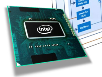
Ivy Bridge (IVB) is the first chip to use Intel's 22nm tri-gate transistors, which will help scale frequency and reduce power consumption. As we already mentioned, mobile Ivy Bridge will be the first Intel CPU to bring four cores into a 35W TDP.
At a high level Ivy Bridge looks a lot like Sandy Bridge. It's still a monolithic die that features an integrated GPU. The entire die is built at 22nm, continuing Intel's march towards truly addressing integrated graphics performance. Ivy Bridge won't get rid of the need for a discrete GPU but, like Sandy Bridge, it is a step in the right direction.
Intel hasn't announced die size but transistor count has increased to approximately 1.4 billion (layout). This is up from 1.16 billion in Sandy Bridge, a 20.7% increase. With perfect scaling a 22nm Sandy Bridge die would be 47.3% the size of a 32nm die. Even with the increase in transistor count, it's a good bet that Ivy Bridge will be noticeably smaller than Sandy Bridge.
Motherboard & Chipset Support
Ivy Bridge is backwards compatible with existing LGA-1155 motherboards, although there will be a new chipset for Ivy Bridge and new motherboards to enable some features (e.g. PCI Express 3.0, native USB 3.0). The new chipset family falls under the 7-series banner. We'll see Z77, Z75, H77, Q77, Q75 and B75 available at or around launch.
| Chipset Comparison | ||||||||
| Z77 | Z75 | H77 | Z68 | P67 | H67 | |||
| CPU Support |
IVB LGA-1155 |
IVB LGA-1155 |
IVB LGA-1155 |
SNB/IVB LGA-1155 |
SNB/IVB LGA-1155 |
SNB/IVB LGA-1155 |
||
| CPU Overclocking | Yes | Yes | No | Yes | Yes | No | ||
| CPU PCIe Config |
1 x16 or 2 x8 or 1 x8 + 2 x4 PCIe 3.0 |
1 x16 or 2 x8 PCIe 3.0 |
1 x16 PCIe 3.0 |
1 x16 or 2 x8 or 1 x8 + 2 x4 PCIe 3.0 |
1 x16 or 2 x8 PCIe 3.0 |
1 x16 PCIe 3.0 | ||
| Processor Graphics Support | Yes | Yes | Yes | Yes | No | Yes | ||
| Intel SRT (SSD caching) | Yes | No | Yes | Yes | No | No | ||
| RAID Support | Yes | Yes | Yes | Yes | Yes | Yes | ||
| USB 2.0 Ports (3.0) | 14 (4) | 14 (4) | 14 (4) | 14 | 14 | 14 | ||
| SATA Total (Max Number of 6Gbps Ports) | 6 (2) | 6 (2) | 6 (2) | 6 (2) | 6 (2) | 6 (2) | ||
| PCIe Lanes | 8 (5GT/s) | 8 (5GT/s) | 8 (5GT/s) | 8 (5GT/s) | 8 (5GT/s) | 8 (5GT/s) | ||
As I mentioned above, Ivy Bridge finally supports USB 3.0 natively. The consumer 7-series chipsets feature 14 total USB ports, 4 of which are USB 3.0 capable. The CPU itself features 16 PCIe (1x16, 2x8 or 1x8 + 2x4) gen 3 lanes to be used for graphics and/or high performance IO. You will only see Gen 3 speeds on qualified motherboards. It's technically possible on 6-series motherboards but guaranteed on 7-series motherboards. The Z77 and H77 chipsets will support Intel's Smart Response Technology (SRT, aka SSD caching) which is a Z68 exclusive today.
SATA and chipset-attached PCIe slots haven't changed. Overclocking is supported on all Z-chipsets, while the H-chipset doesn't. All chipsets support Intel's HD Graphics, which is a departure from the Sandy Bridge mess where P67 didn't.


97 Comments
View All Comments
driscoll42 - Saturday, September 17, 2011 - link
On the last page there's "Should the fab engineers at Intel do their job well, Ivy Bridge could deliver much better power characteristics than Ivy." in the second paragraph, should that be Sandy on the end?Anand Lal Shimpi - Saturday, September 17, 2011 - link
Thank you! Fixed :)Take care,
Anand
Beenthere - Saturday, September 17, 2011 - link
It's good that Intel has decided that their GPU sucks and that to be competitive they need to catch up to AMD. This will take some time as AMD has a two year head start on APUs but it's all good for consumers.In spite of the marketing hype from Intel it looks like they've conceded that AMD has the better system approach with APUs for mainstream consumers and laptops. CPU performance alone is no longer a valid yardstick for PC performance thanks to AMD's advance thinking and Llano.
TypeS - Saturday, September 17, 2011 - link
I realize Intel is behind (has been for since anyone can remember) in the graphics arena compared to AMD/ATI and NVIDIA, but is AMD "two years ahead" in terms of an APU? While Clarkdale can't really be considered a true all in one package (hey remember when Kentsfield wasn't considered a true quad core?), it was still an all in one package, and with Sandy Bridge, Intel brought it all together onto one die. Intel isn't calling it an APU but if you compare SNB and Llano/Bulldozer, they share some similarities.AMD's edge is on graphics, and Intel is closing the gap.
I might be missing something though in why you say they are ahead in terms of an "APU", but from my knowledge, Intel as first to release a retail/commercial APU.
Guspaz - Monday, September 19, 2011 - link
Intel might be catching up in terms of physical performance, but Intel's drivers still, quite frankly, suck. It's the one thing really holding the platform back, in terms of both compatibility and performance. Even simple things like flash acceleration can sometimes be wonky with Intel's drivers.Furthermore, developers like Carmack have been pestering Intel to give them lower-level access to the hardware, with potentially enormous performance benefits; they'd like to treat PCs more like a console, and stripping away much of the driver/graphics overhead (particularly in terms of memory management) could see some pretty big performance gains. There's a reason why modern integrated GPUs like in Ivy Bridge have theoretical performance on-par with a 360 or PS3, but in practice, are nowhere near as performant.
Of course, the same is true for AMD and nVidia; high-end developers like Carmack and Sweeney seem to want lower-level access to hardware. From Carmack's latest QuakeCon keynote, it does seem like the hardware manufacturers are listening.
fic2 - Monday, September 19, 2011 - link
Yeah, Intel seems to want to catch up and made a pretty decent effort of no sucking with the HD3000. BUT then they go and do a dumb@ss thing like put the crappy HD2000 on 90% of the Sandies they sell. I think if marketing would get the he11 out of the way they wouldn't be too sucky.Oh, yeah, except the drivers.
bigboxes - Saturday, September 17, 2011 - link
I love AMD as much as the next guy (have three running AMD boxes), but are you going to continue to be "that guy" that posts this nonsense in every Intel/AMD thread? We get it. You love AMD and want to help them win the CPU wars. Yay for fanbois everywhere!Beenthere - Saturday, September 17, 2011 - link
Intel hasn't released an APU. They have released a CPU and GPU on the same slab of silicon. That's not an integrated APU.No nonsense, just facts. I like facts. Some folks can't handle facts but that's life. I like choice and scrupulous businesses. That's what AMD is unlike Intel.
ltcommanderdata - Saturday, September 17, 2011 - link
For someone arguing against marketing hype and looking for facts you seem overly preoccupied by AMD's APU term. If you are looking for which product currently on the market has tighter CPU/IGP integration then that produce is Sandy Bridge not Llano. For instance Sandy Bridge allows bidirectional communication/sharing of instructions and data between the CPUs and IGP via a shared on die L3 cache instead of through a crossbar and off die system memory as in Llano. Sandy Bridge also has more advanced power and thermal monitoring allowing efficient sharing of TDP room between the CPU and IGP, allowing each to be overclocked as needed, something Llano doesn't do.Yes, Llano has the faster GPU, but that's not the critical concern if what you are interested in is integration. Intel's CPU and GPU on a slab of silicon was Arrandale. Sandy Bridge has moved well beyond that. Llano's CPU/GPU integration looks to be somewhere in between Arrandale and Sandy Bridge. Seeing Llano is AMD's 1st generation Fusion product along with Brazos that's fine. But just because AMD's calls their product an APU doesn't mean it's the pinnacle of CPU/GPU integration.
gramboh - Sunday, September 18, 2011 - link
Boom. Beenthere just got roasted, and of course disappears rather than admitting he was wrong.