Kal-El Has Five Cores, Not Four: NVIDIA Reveals the Companion Core
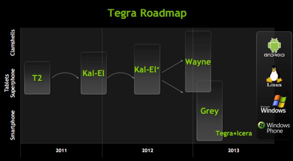
by Anand Lal Shimpi on September 20, 2011 11:46 AM ESTLast week NVIDIA provided an update on its Tegra SoC roadmap. Kal-El, its third generation SoC (likely to launch as Tegra 3) has been delayed by a couple of months. NVIDIA originally expected the first Kal-El tablets would arrive in August, but now it's looking like sometime in Q4. Kal-El's successor, Wayne, has also been pushed back until late 2012/early 2013. In between these two SoCs is a new part dubbed Kal-El+. It's unclear if Kal-El+ will be a process shrink or just higher clocks/larger die on 40nm.
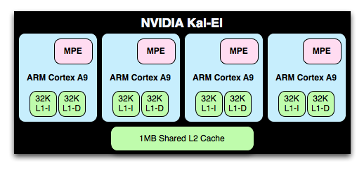
In the smartphone spirit, NVIDIA is letting small tidbits of information out about Kal-El as it gets closer to launch. In February we learned Kal-El would be NVIDIA's first quad-core SoC design, featuring four ARM Cortex A9s (with MPE) behind a 1MB shared L2 cache. Kal-El's GPU would also see a boost to 12 "cores" (up from 8 in Tegra 2), but through architectural improvements would deliver up to 3x the GPU performance of T2. Unfortunately the increase in GPU size and CPU core count doesn't come with a wider memory bus. Kal-El is still stuck with a single 32-bit LPDDR2 memory interface, although max supported data rate increases to 800MHz.
We also learned that NVIDIA was targeting somewhere around an 80mm^2 die, more than 60% bigger than Tegra 2 but over 30% smaller than the A5 in Apple's iPad 2. NVIDIA told us that although the iPad 2 made it easier for it to sell a big SoC to OEMs, it's still not all that easy to convince manufacturers to spend more on a big SoC.
Clock speeds are up in the air but NVIDIA is expecting Kal-El to run faster than Tegra 2. Based on competing A9 designs, I'd expect Kal-El to launch somewhere around 1.3 - 1.4GHz.
Now for the new information. Power consumption was a major concern with the move to Kal-El but NVIDIA addressed that by allowing each A9 in the SoC to be power gated when idle. When a core is power gated it is effectively off, burning no dynamic power and leaking very little. Tegra 2 by comparison couldn't power gate individual cores, only the entire CPU island itself.
In lightly threaded situations where you aren't using all of Kal-El's cores, the idle ones should simply shut off (if NVIDIA has done its power management properly of course). Kal-El is built on the same 40nm process as Tegra 2, so when doing the same amount of work the quad-core chip shouldn't consume any more power.
Power gating idle cores allows Kal-El to increase frequency to remaining active cores resulting in turbo boost-like operation (e.g. 4-cores active at 1.2GHz or 2-cores at 1.5GHz, these are hypothetical numbers of course). Again, NVIDIA isn't talking about final clocks for Kal-El or dynamic frequency ranges.
Five Cores, Not Four
Courtesy NVIDIA
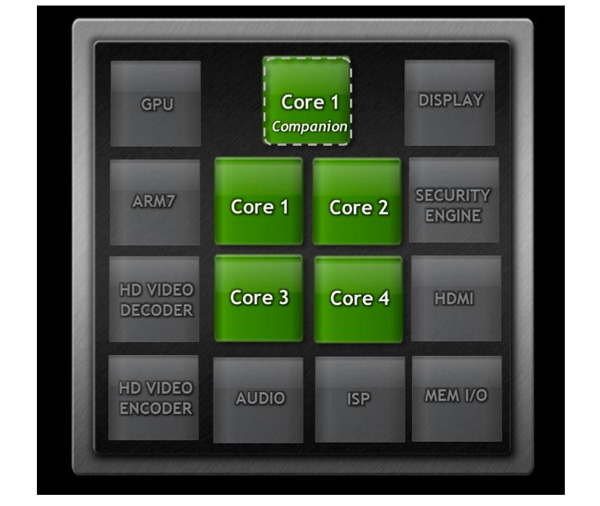
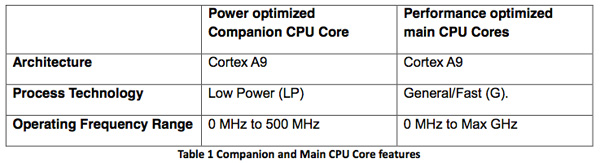
Finally we get to the big news. There are actually five ARM Cortex A9s with MPE on a single Kal-El die: four built using TSMC's 40nm general purpose (G) process and one on 40nm low power (LP). If you remember back to our Tegra 2 review you'll know that T2 was built using a similar combination of transistors; G for the CPU cores and LP for the GPU and everything else. LP transistors have very low leakage but can't run at super high frequencies, G transistors on the other hand are leaky but can switch very fast. Update: To clarify, TSMC offers a 40nm LPG process that allows for an island of G transistors in a sea of LP transistors. This is what NVIDIA appears to be using in Kal-El, and what NV used in Tegra 2 prior.
The five A9s can't all be active at once, you either get 1 - 4 of the GP cores or the lone LP core. The GP cores and the LP core are on separate power planes.
NVIDIA tells us that the sole point of the LP Cortex A9 is to provide lower power operation when your device is in active standby (e.g. screen is off but the device is actively downloading new emails, tweets, FB updates, etc... as they come in). The LP core runs at a lower voltage than the GP cores and can only clock at up to 500MHz. As long as the performance state requested by the OS/apps isn't higher than a predetermined threshold, the LP core will service those needs. Even with your display on it's possible for the LP core to be active, so long as the performance state requested by the OS/apps isn't too high.
Courtesy NVIDIA
Once it crosses that threshold however, the LP core is power gated and state is moved over to the array of GP cores. As I mentioned earlier, both CPU islands can't be active at the same time - you only get one or the other. All five cores share the same 1MB L2 cache so memory coherency shouldn't be difficult to work out.
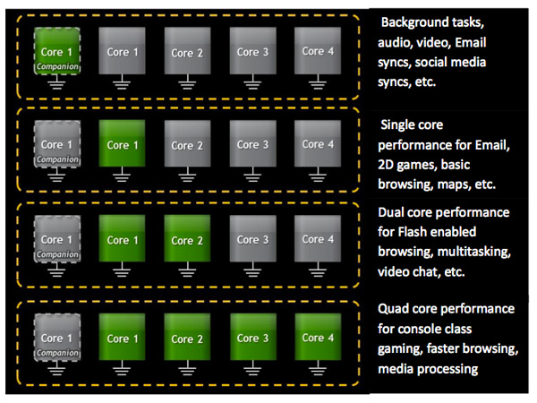
Android isn't aware of the fifth core, it only sees up to 4 at any given time. NVIDIA accomplishes this by hotplugging the cores into the scheduler. The core OS doesn't have to be modified or aware of NVIDIA's 4+1 arrangement (which it calls vSMP). NVIDIA's CPU governor code defines the specific conditions that trigger activating cores. For example, under a certain level of CPU demand the scheduler will be told there's only a single core available (the companion core). As the workload increases, the governor will sleep the companion core and enable the first GP core. If the workload continues to increase, subsequent cores will be made available to the scheduler. Similarly if the workload decreases, the cores will be removed from the scheduling pool one by one.
Courtesy NVIDIA
NVIDIA can switch between the companion and main cores in under 2ms. There's also logic to prevent wasting time flip flopping between the LP and GP cores for workloads that reside on the trigger threshold.
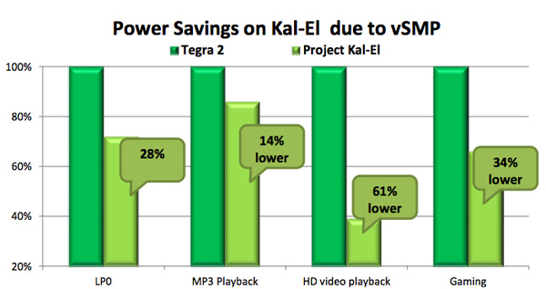
NVIDIA expects pretty much all active work to be done on the quad-core GP array, it's really only when your phone is idle and dealing with background tasks that the LP core will be in use. As a result of this process dichotomy NVIDIA is claiming significant power improvements over Tegra 2, despite an increase in transistor count:
Courtesy NVIDIA
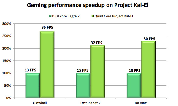
NVIDIA isn't talking about GPU performance today but it did reveal a few numbers in a new white paper:
Courtesy NVIDIA
We don't have access to the benchmarks here but everything was run on Android 3.2 at 1366 x 768 with identical game settings. The performance gains are what NVIDIA has been promising, in the 2 - 3x range. Obviously we didn't run any of these tests ourselves so approach with caution.
Final Words
What sold NVIDIA's Tegra 2 wasn't necessarily its architecture, but timing and the fact that it was Google's launch platform for Honeycomb. If the rumors are correct, NVIDIA isn't the launch partner for Ice Cream Sandwich, which means Kal-El has to stand on its own as a convincing platform.
Courtesy NVIDIA
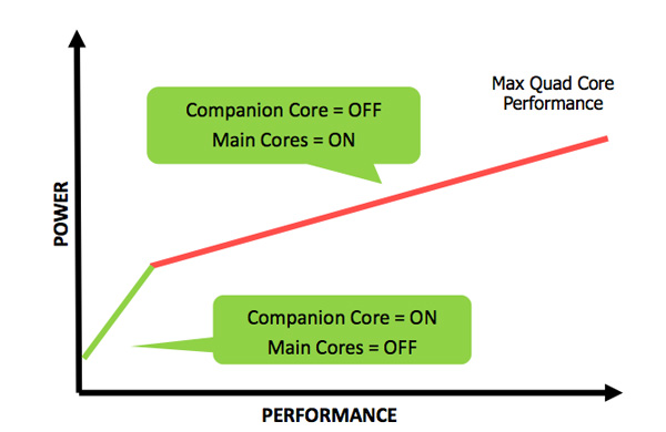
The vSMP/companion core architecture is a unique solution to the problem of increasing SoC performance while improving battery life. This is a step towards heterogenous multiprocessing, despite the homogenous implementation in Kal-El. It remains to be seen how tangible is the companion core's impact on real world battery life.


74 Comments
View All Comments
polysick - Wednesday, September 21, 2011 - link
Don't you think having the 5 core setup is more impressive than hkmg? The idea is you are only going to be running a single core most of the time anyway.Wolfpup - Wednesday, September 21, 2011 - link
A year ago we were using A8, and in fact that's still what's in Apple's stuff, and A8 isn't remotely fast enough. The dual core A9 @ 1Ghz seems to run single threaded stuff pretty well, though it's still slower than I'd like, and we're still running very crippled OSes.Gauner - Tuesday, September 20, 2011 - link
I actually would like to see something similar in desktop architectures, I usually buy high end quad cores for work(3d rendering and video editing/compression), but it has always seem a little wasteful to use that as main desktop computer, most of the time my PC is only doing simple tasks like irc, web browsing, playing music/movies, ... and I think I'm not the only one that wastes energy with quad cores most of the time.A extra core with an atom or low end llano would be perfect for that, you could let the 10w cpu work most of the time, and only wake up the 80+W quad core when needed, in a year it should give some nice savings in energy. And yes, I know that those 80-100w are only consumed under full load, but I doubt a i7 2600k will consume 10 or 15w or less with only simple task in the background.
Mike1111 - Tuesday, September 20, 2011 - link
The Cortex-A9's companion core role sounds a lot like the dual-core Cortex-M4's in OMAP5 (in addition to the dual-core Cortex-A15). Just 9 months earlier :-)I'm wondering if Apple's gonna do something similar for the CPU in the A6, since spring 2012 seems to be to early for a full-blown quad-core Cortex-A15 and I can't see them going quad-core Cortex-A9 like Nvidia.
z0mb13n3d - Tuesday, September 20, 2011 - link
The idea is similar, but the execution is different, very different. The M4's in the OMAP5 can run (or support) very specific tasks that have to do with the video decode, ISP etc, while the main A15's are running. They are not general purpose cores. As listed in the article above, processes such as background sync (email, FB etc.) or any 'general purpose' Android code execution will wake up the A15's in OMAP5.In this case however, the 'companion' (definitely could have come up with a better term for this) core in Kal-El is a full-blown general purpose low-power A9 core , that is capable of running everything the other 4 A9 cores can, albeit significantly slower and only up to a certain utilization threshold (for obvious performance reasons). So in effect, unless utilization spikes, the 4 'main' cores would probably never wake up while the device is in standby.
Although I'm not sure how accurate the numbers nvidia provided are (definitely seem optimistic), if it's true that the companion core does in fact have the MPE block, I can understand the HD video playback power savings claims. Doesn't Flash also use MPE to an extent?
ltcommanderdata - Tuesday, September 20, 2011 - link
Given everyone seemed to standardize on 512kB of L2 cache for the Cortex A8, which then carried over as 512kB L2 cache per core for for dual core Cortex A9 SoCs, is there any performance concerns now that 4 cores are having to share the same 1MB L2 cache?polysick - Wednesday, September 21, 2011 - link
I would think there shouldn't be. When a single of the GP cores gets activated, it would seem that clock rate increases (if I read that correctly), which makes sense since with the smaller area you have to worry less about clock skew. This is AKA the 'turbo boost' mentioned. So if you have 4 cores active, I think you would have a slower clock rate, so maybe L2 cache congestion wouldn't be as much of an issue?macs - Tuesday, September 20, 2011 - link
Anand, I would love an article that summarize what is expected to be available in the coming months/year (OMAP 5,Kal-el,Krait, Exynos quad core, A6)...We need more order in this SOC world because it has a lot of players!
Blaster1618 - Friday, September 23, 2011 - link
I second that request, When I read your original article on Nvidia's road map I thought they were going to sweep the market, but in that time it seems like TI and the other competitors have raised their SOC game 2-3 orders of magnitude, I'm lov'n it. Samsung information is always sketchy until there months from release. I tried once to look through ARM's customer list and quickly got a headache. B-)SniperWulf - Tuesday, September 20, 2011 - link
I think its cool that nvidia appears to be progressing nicely in the ARM world. But since they are still primarily a graphics company, I really expected the T3 (or whatever it will be called) to blow the doors off of Mali and A5