The iPad 2,4 Review: 32nm Brings Better Battery Life
by Anand Lal Shimpi on May 4, 2012 12:50 AM ESTWhen Apple launched the 3rd generation iPad (as the new iPad), it also dropped the price of the entry-level 16GB WiFi iPad 2 to $399. Apple's products tend to hold their values exceptionally well, so this two-tablet strategy made sense. Apple also proved the success of discount-the-previous-gen strategy with its iPhone line, where you can now buy current, n-1 and n-2 generations of iPhones at prices separated by $100.
What's different with the $399 iPad 2 is that Apple used it as a vehicle to introduce a new hardware platform, or more specifically, a new SoC.
The 32nm HK+MG Apple A5 SoC
Prior to the new iPad announcement there were three versions of the iPad 2:
| Apple iPad 2 Lineup | |||||||
| iPad 2,1 | iPad 2,2 | iPad 2,3 | iPad 2,4 | ||||
| A5 SoC | 45nm LP | 45nm LP | 45nm LP | 32nm LP | |||
| Connectivity | WiFi | WiFi + GSM | WiFi + CDMA | WiFi | |||
The 2,1 was WiFi-only, the 2,2 was GSM and the 2,3 was CDMA. The new addition to the family is the iPad 2,4. The 2,4 replaces the original iPad 2,1. It's also only available in a single capacity.
There's no known way to tell whether you're getting an iPad 2,4 vs. the older iPad 2,1 without opening the box. The 2,4 unit I ended up with was made in China, ruling out manufacturing region as a way of telling. The external box looks identical, as does the device itself.
The newer iPad 2,4 units should come with iOS 5.1 preloaded, while any older iPad 2,1 stock may have 5.0.1 or older. But the most accurate way to tell is by looking at what a utility like Geekbench will tell you about the hardware (Update: there are other free utilities that can serve the same purpose, Linpack and Battery Life Pro are two examples):
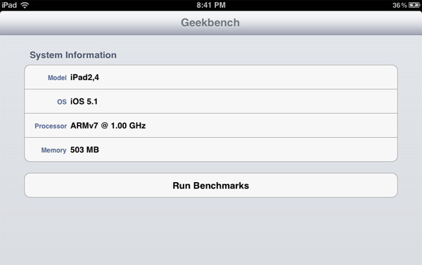
This particular iPad 2,4 sample came from Best Buy, and several attempts to find one elsewhere came up short. All indications seem to point to the iPad 2,4 being relatively rare, which makes sense considering what's inside it.
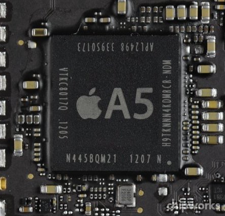
Although the iPad 2,1 and its 3G brethren all used a 45nm Apple A5 SoC, the iPad 2,4 uses a die-shrunk 32nm version. The performance remains the same, but the die is much smaller. This isn't however just a normal die shrink, as Apple is using Samsung's 32nm high-k + metal gate LP transistors for this new A5 die. Intel was first to make the HK+MG transition back at 45nm in 2007 and correctly predicted that no one else would make the move until 32nm at the earliest.
Transistors are amazingly complex to fully understand, but at a high level they're quite simple. Imagine a transistor as a silicon based switch. When on, current flows, and when off, current stops flowing. The smaller you make a transistor, the more likely it is to misbehave. If current flows while the transistor is off, you waste power. This is known as leakage current and can come from a number of sources.
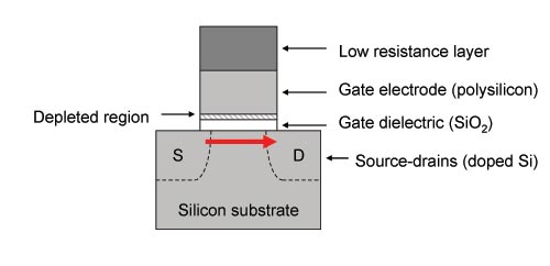
One such source is the gate oxide/gate dielectric, a particularly thin part of modern day transistors - on the order of a handful of atoms thick. Thinning the gate dielectric is desirable up to a certain point, after which the dielectric simply leaks too much power. Switching to a different material here, specifically one with a higher dielectric constant (a higher k-value), can significantly reduce leakage current and mitigate this issue. This is exactly what the first part of Samsung's 32nm high-k + metal gate process does.
The second half of the new process is the introduction of a metal gate electrode. Switching from a polysilicon to a metal gate electrode results in higher drive current by elimination of a region of depleted conducting carriers between the gate electrode and gate dielectric.
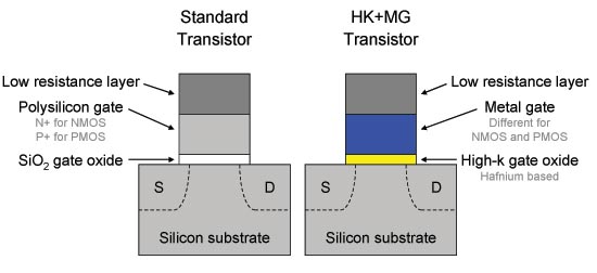
The combination of these two innovations results in less wasted current and more efficient current delivery, which in turn can give us a more power efficient chip. It's a net win. It makes manufacturing more complex, and there's definitely a learning curve to implementing it, but after you get over that hurdle it becomes just another part of the process.
The More Cost Effective Die
Traditionally the move to a smaller process node brings about an increase in transistor density. As transistors get smaller, you can fit more of them into the same space (or the same number into a smaller space). It's this basic principle that makes Moore's Law work. If you can keep shrinking transistor size by about 50% every two years, you'll theoretically be able to double transistor count at the same cost every two years (or cut cost in half every two years). In practice it doesn't work this well. Newer processes are always more expensive than their predecessors initially and logic scaling is never perfect.
It's rare these days that we actually see a pure die shrink anymore. With Intel's tick-tock model we almost always see increases in functionality to accompany each process node shift. In the case of Ivy Bridge, we actually saw a significant increase in transistor count thanks to an improved GPU. With Apple's 32nm A5 however, we truly end up with a die shrunk version of the 45nm A5 SoC. About the only part of the computing world where we see these pure shrinks is in the console space where performance doesn't have to go up within a generation, but cost must go down.
45nm A5 (left) vs. 32nm A5 (right) - Source: Chipworks
The original 45nm A5's die measured approximately 122mm^2. The new 32nm A5 has a surface area of only 69mm^2. That's actually amazingly good scaling at 57% of the old die size, as perfect scaling from 45nm to 32nm would be around 50.5%.
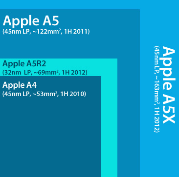
Assuming Apple could make full use of a 300mm wafer (which it can't, wafers are round, chips are rectangular at best so there are some unusable chips), Samsung could deliver 579 45nm A5 die to Apple. The move to 32nm would give Apple 75% more die per wafer at 1015 chips. Again both of these numbers are over estimates as they assume full usage of the surface area of a wafer as well as 100% yields, but you can see the benefit of a smaller die. As long as wafer costs increase by a factor less than the 75% increase in number of die per wafer, Apple can effectively reduce SoC cost by going this route.
These ARM based SoCs are already fairly cheap - all selling well below $30 (many around $15) - so there's not a whole lot of cost savings here. On a product like the $399 iPad 2, where Apple needs to do its best to maintain margins while holding onto (and growing) market share, every last dollar matters.
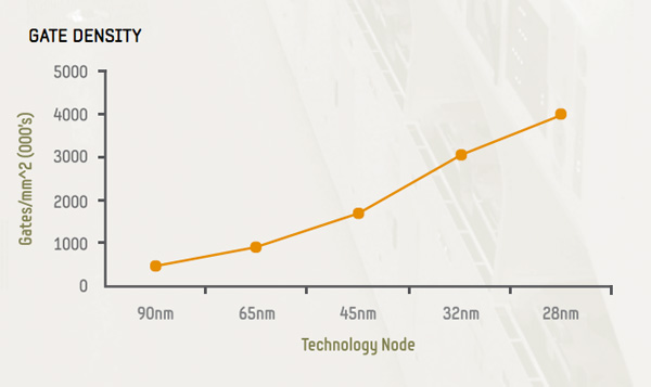
Gate density vs. process node at Samsung
There's another motivation for Apple however. Just as with any good microprocessor company, its best to introduce a new process technology on a known architecture. It's also a good idea to introduce a new process technology on lower volume products. The combination of both of these minimize risk. Should there be something wrong with the new process, introducing a new architecture on it just means you now have two very complex things to debug - the process technology and the chip's architecture. Should the new process not yield very well initially, you'd be similarly screwed if you were depending on it for your highest volume parts.
32nm A5 in iPad 2,4 (Source: Chipworks)
Apple decided to try out Samsung's 32nm HK+MG process on the A5 used in the 3rd generation Apple TV and some of the new iPad 2s. The former is a relatively low volume product for Apple, while the latter still moves in significant quantities. To deal with that fact, Apple is continuing to ship the original 45nm iPad 2,1 alongside the new 32nm iPad 2,4. Any hiccups in Samsung's production of the A5 and there are still more than enough iPad 2,1s to go around. The risk of moving to 32nm is effectively mitigated, while the learnings Apple gains from building the 32nm A5 will pay off later this year as Apple ramps up production of a 32nm SoC for use in the next iPhone. It's a very smart strategy, one you would expect from an experienced chip company - not a device vendor. When you consider that Apple employs chip architects who have worked on everything from the Athlon 64 to the Cortex A15, Apple's behavior is no longer that surprising.
Apple gets two benefits from the iPad 2,4: lower manufacturing costs, and experience with Samsung's 32nm HK+MG process which it will later use in much greater volumes. What about customers who end up with an iPad 2,4? Better battery life and cooler operation, of course.
Impact of HK+MG at Samsung
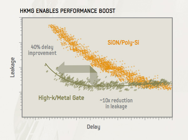
Remember the basics of Samsung's 32nm HK+MG process: a 40% performance improvement at the same leakage, or a 10x reduction in leakage at the same switching speed. As the iPad 2,4 retains the same clocks as the initial iPad 2, the benefit realized is a significant reduction in leakage current. This translates to tangibly better battery life.


100 Comments
View All Comments
PeteH - Friday, May 4, 2012 - link
Was video testing done full screen or letterboxed? Assuming it was done letterboxed, is it possible that backlighting of the display can be selectively turned off near the top and bottom of the screen? That would definitely save power.It'd be easy enough to test. Just run the test full screen and see if the playback time changes.
dagamer34 - Monday, May 7, 2012 - link
Backlight works across the entire display. There is no local dimming.jjj - Friday, May 4, 2012 - link
Not so sure the foundry part is working all that well,they didn't had 32nm for the ipad 3 and they had to cut a few corners without it (huge battery- ads cost , weight and bulk , way hotter , moving the ram on the other side of the PCB ).You put a positive spin on the way they transitioned to 32nm but there is no reason to keep the 32nm part low vol,and not transition all ipad 2 SKUs if Samsung has capacity and yields are good so something might not be quite there just yet. I always thought the ipad 3 on 45nm was a plan B device and Apple having A5 on 32nm this early makes it look even more so.
BSMonitor - Friday, May 4, 2012 - link
Sure there is. Apple has no control of the volume for the A5X if they have TSMC move to a new node and try and build a new SoC on it. We have seen ALL CPU/GPU manufacturers struggle with yield when transitions to new nodes coincide with new designs. So rather risk holding back 30 million iPad 3's to a April, May, June launch, they took the risk of low yields out of the equation and stuck with 45nm.Remember, any transition to a new node for any chip maker is typically a different Fab. And/or retooling existing Fabs. So as new 32nm Fab's come online, they won't be anywhere near the capacity of 45nm Fab's for some time.
We don't mention this much, because Intel has made this seem almost immaterial. But it is a BIG deal, and VERY expensive to ramp new nodes. Look at AMD, this side of the game would have eventually bankrupted them due to the expense of it all.
BSMonitor - Friday, May 4, 2012 - link
Err. Samsung not TSMC.. LOLltcommanderdata - Friday, May 4, 2012 - link
It's not just the iPad 3 that would find a 32nm shrink useful. With it's higher battery consumption, it's interesting that Apple didn't decide to use the 3G iPad 2 as the 32nm A5 testbed. The 3G iPad 2 is also presumably a lower volume product than the WiFi iPad 2 which also works in it's favour as a pilot. Would an SoC change still require a new round of carrier/government radiation testing, since that would be a major disincentive?It's good that you found the performance of the iPad2,4 unchanged. Your previous new AppleTV articles mentioned that it was coupled with a single 512MB LPDDR2 RAM die indicating only a single 32-bit channel memory configuration. It looks like the 32nm A5 in the iPad 2,4 implements the full 2x64-bit memory system.
Given the smartphone GPU performance showing in the Exynos 4412, if Apple wants to regain the GPU performance crown and hold it into 2013 when Rogue shows up, they'll probably need to be more aggressive than an up-clocked 32nm A5 in the iPhone 5. The 32nm A5 looks like a shoe-in for the next iPod Touch though.
André - Friday, May 4, 2012 - link
Why?Everything in iOS is synced to 60Hz, which SGX543MP2 already does at 960 x 640.
Sure you could always add more eye candy.
gevorg - Friday, May 4, 2012 - link
Not sure why Apple would be so conservative about rolling out the 32nm process with such a limited run for more than half of 2012, while Samsung just released their Galaxy S3 build on 32nm and ready to sell like hotcakes.KoolAidMan1 - Friday, May 4, 2012 - link
Apple is selling every single iPad that they make. Potential supply constraints from a new process is a huge risk to take. Low initial yields are a common bottleneck for new products, look at what is happening with the GTX 680 right now.They weighed the pros and cons and decided to go with what is proven, tradeoff being the absolutely massive A5X SoC.
Also note that new iPad production started late last year. Just a few months makes quite a difference, which is why we'll soon be seeing 32nm in upcoming smartphones.
BSMonitor - Friday, May 4, 2012 - link
Actually, the Galaxy S3 accounts for a fraction of the new Ipads necessary for its launch.