ARM's Cortex A57 and Cortex A53: The First 64-bit ARMv8 CPU Cores
by Anand Lal Shimpi on October 30, 2012 11:58 AM EST- Posted in
- CPUs
- IT Computing
- Arm
- Cloud Computing
- SoCs
Yesterday AMD revealed that in 2014 it would begin production of its first ARMv8 based 64-bit Opteron CPUs. At the time we didn't know what core AMD would use, however today ARM helped fill in that blank for us with two new 64-bit core announcements: the ARM Cortex-A57 and Cortex-A53.
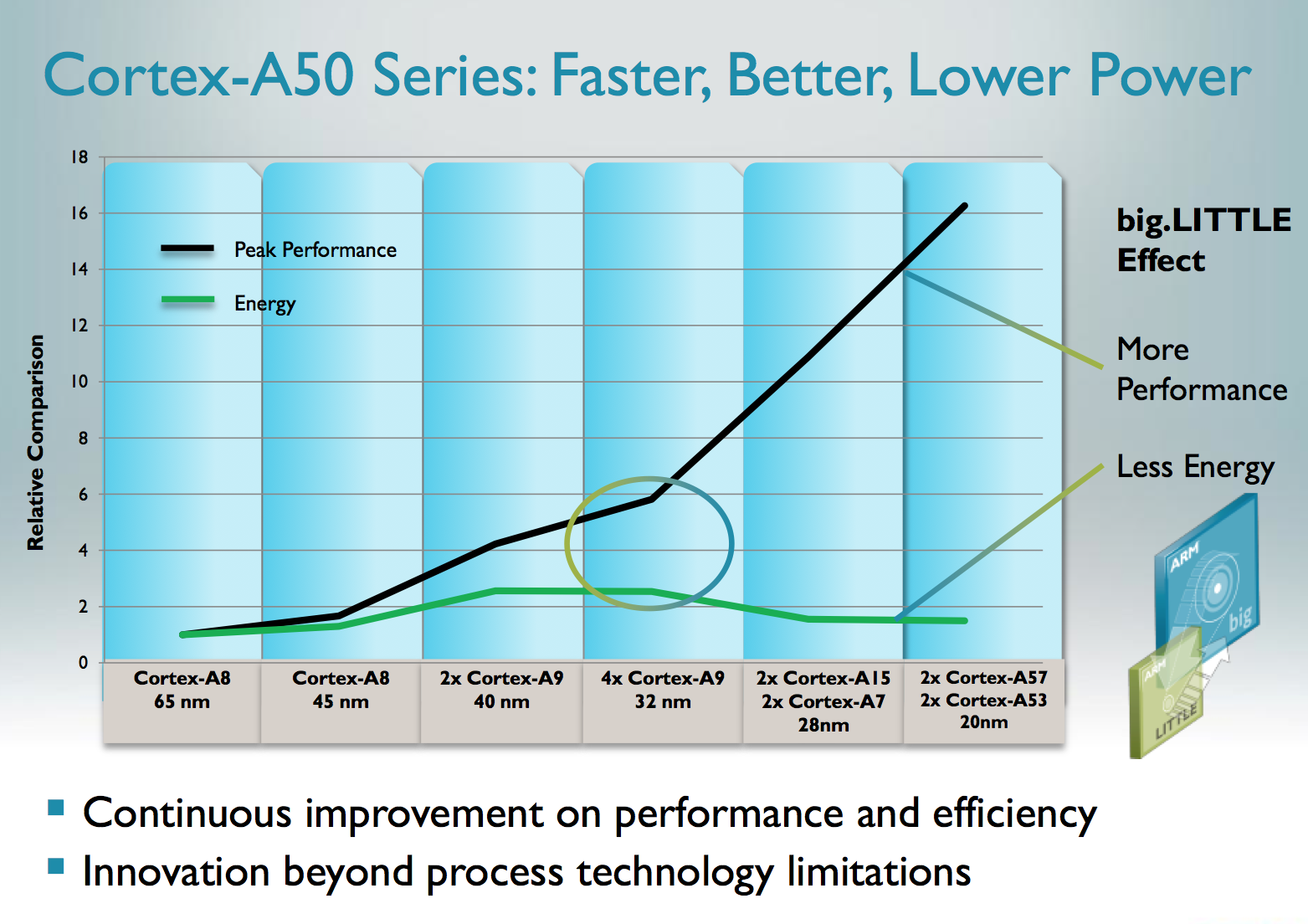
You may have heard of ARM's Cortex-A57 under the codename Atlas, while A53 was referred to internally as Apollo. The two are 64-bit successors to the Cortex A15 and A7, respectively. Similar to their 32-bit counterparts, the A57 and A53 can be used independently or in a big.LITTLE configuration. As a recap, big.LITTLE uses a combination of big (read: power hungry, high performance) and little (read: low power, lower performance) ARM cores on a single SoC.

By ensuring that both the big and little cores support the same ISA, the OS can dynamically swap the cores in and out of the scheduling pool depending on the workload. For example, when playing a game or browsing the web on a smartphone, a pair of A57s could be active, delivering great performance at a high power penalty. On the other hand, while just navigating through your phone's UI or checking email a pair of A53s could deliver adequate performance while saving a lot of power. A hypothetical SoC with two Cortex A57s and two Cortex A53s would still only appear to the OS as a dual-core system, but it would alternate between performance levels depending on workload.
 ARM's Cortex A57
Architecturally, the Cortex A57 is much like a tweaked Cortex A15 with 64-bit support. The CPU is still a 3-wide/3-issue machine with a 15+ stage pipeline. ARM has increased the width of NEON execution units in the Cortex A57 (128-bits wide now?) as well as enabled support for IEEE-754 DP FP. There have been some other minor pipeline enhancements as well. The end result is up to a 20 - 30% increase in performance over the Cortex A15 while running 32-bit code. Running 64-bit code you'll see an additional performance advantage as the 64-bit register file is far simplified compared to the 32-bit RF.
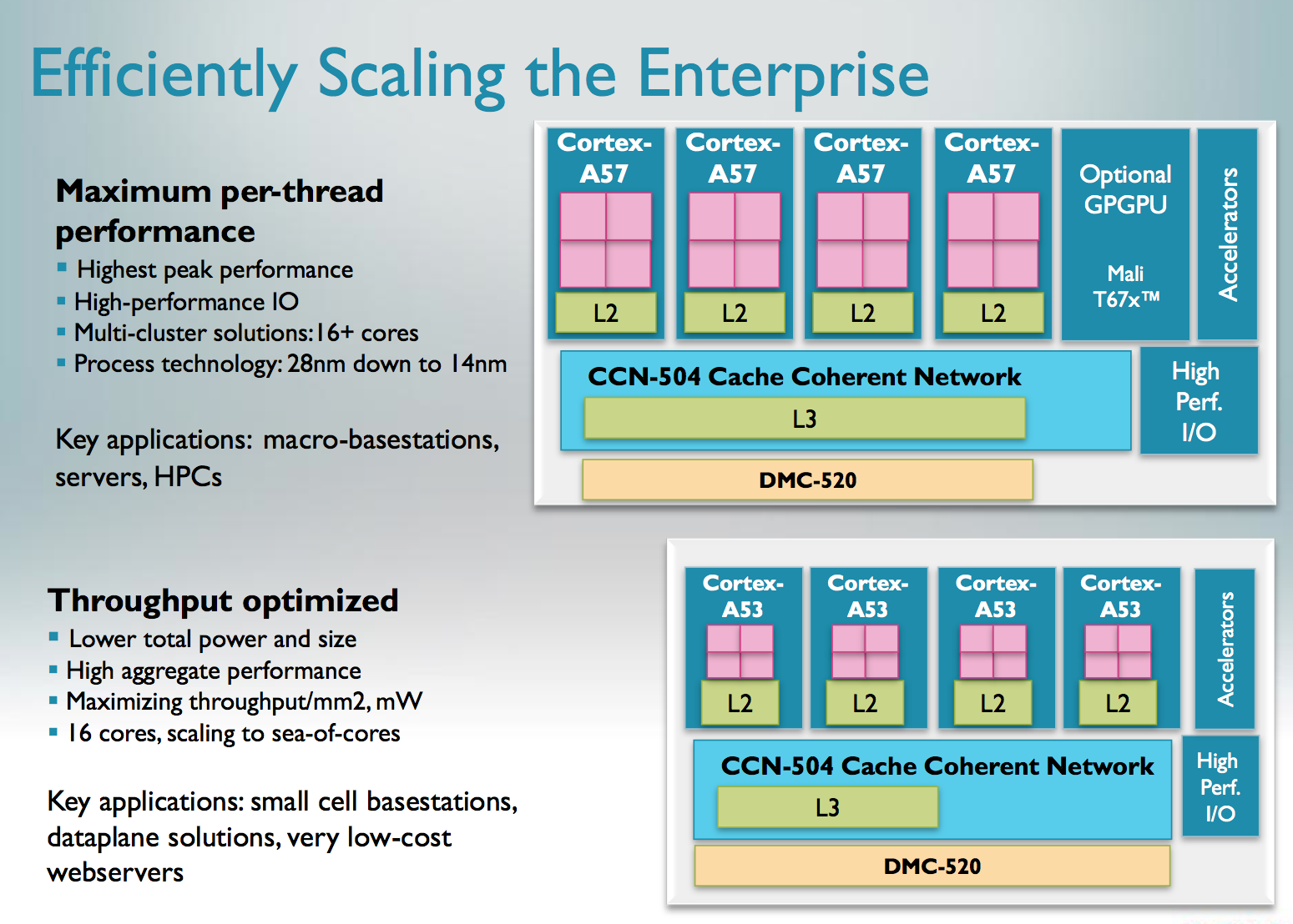
The Cortex A57 will support configurations of up to (and beyond) 16 cores for use in server environments. Based on ARM's presentation it looks like groups of four A57 cores will share a single L2 cache.
ARM's Cortex A53
Similarly, the Cortex A53 is a tweaked version of the Cortex A7 with 64-bit support. ARM didn't provide as many details here other than to confirm that we're still looking at a simple, in-order architecture with an 8 stage pipeline. The A53 can be used in server environments as well since it's ISA compatible with the A57.
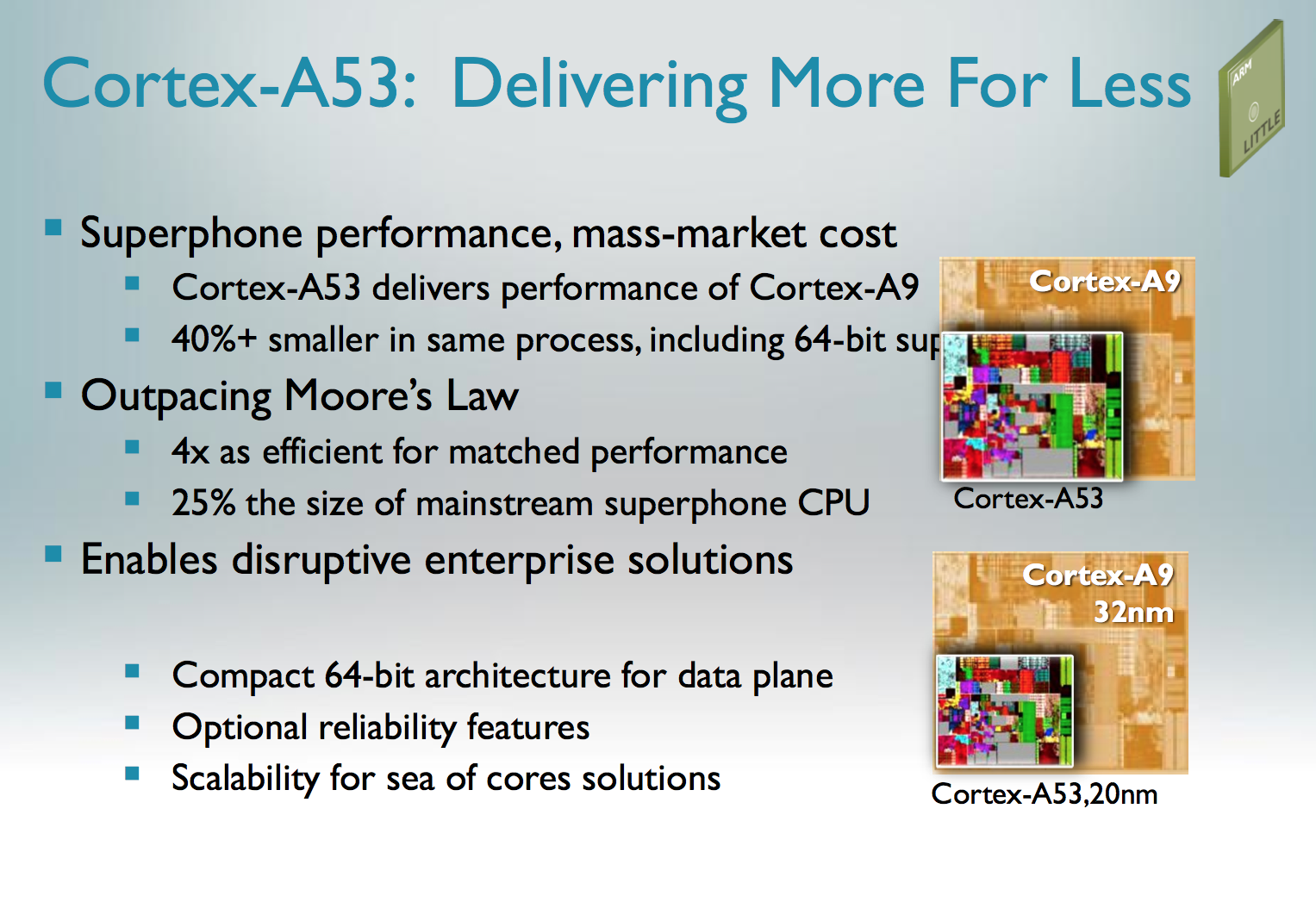
ARM claims that on the same process node (32nm) the Cortex A53 is able to deliver the same performance as a Cortex A9 but at roughly 60% of the die area. The performance claims apply to both integer and floating point workloads. ARM tells me that it simply reduced a lot of the buffering and data structure size, while more efficiently improving performance. From looking at Apple's Swift it's very obvious that a lot can be done simply by improving the memory interface of ARM's Cortex A9. It's possible that ARM addressed that shortcoming while balancing out the gains by removing other performance enhancing elements of the core.
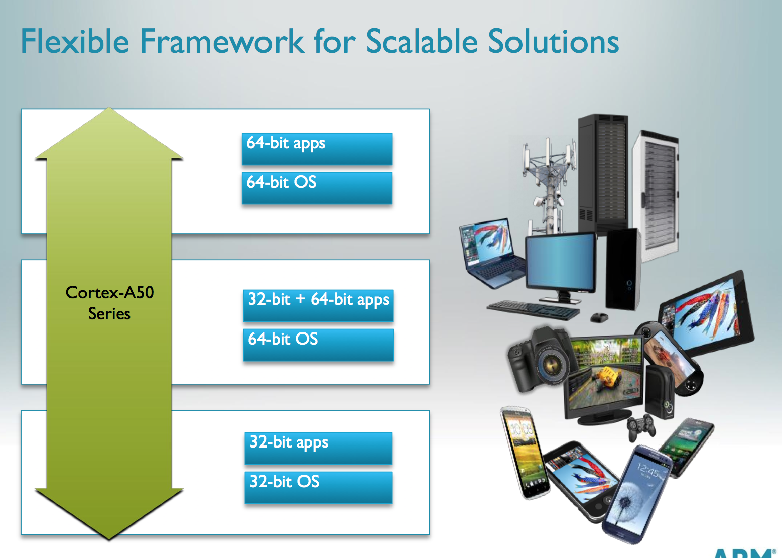
Both CPU cores are able to run 32-bit and 64-bit ARM code, as well as a mix of both so long as the OS is 64-bit.
Completed Cortex A57 and A53 core designs will be delivered to partners (including AMD and Samsung) by the middle of next year. Silicon based on these cores should be ready by late 2013/early 2014, with production following 6 - 12 months after that. AMD claimed it would have an ARMv8 based Opteron in production in 2014, which seems possible (although aggressive) based on what ARM told me.
ARM expects the first designs to appear at 28nm and 20nm. There's an obvious path to 14nm as well.
It's interesting to note ARM's commitment to big.LITTLE as a strategy for pushing mobile SoC performance forward. I'm curious to see how the first A15/A7 designs work out. It's also good to see ARM not letting up on pushing its architectures forward.


117 Comments
View All Comments
Heisenburger - Tuesday, October 30, 2012 - link
"ARM is definitely more interesting at the moment."Because that's where all the buzz is at: smartphones and tablets.
BSMonitor - Tuesday, October 30, 2012 - link
Because that's where people with money and no knowledge see "new" profits..listic - Tuesday, October 30, 2012 - link
"reducing power every year"? Not so much, in my humble opinion.Look where Intel was in 2004:
http://ark.intel.com/products/27609
http://en.wikipedia.org/wiki/List_of_Intel_Pentium...
Pentium M ULV 733 processor, released in July 20, 2004, had TDP of 5W.
Sure, nowadays you get multi-core, hyper-threading, memory controller and integrated graphics on-chip, but the lowest power you can buy (apart from Atom) has 17W TDP. That doesn't count as reducing power in my books. Surely, some stagnation is there.
andrewaggb - Tuesday, October 30, 2012 - link
Those are slightly different things. Well performance/watt has generally improved with every tick/tock.But overall TDP has been improving with ivy bridge and supposedly haswell. Their new atom designs have pretty good TDP as well.
I get what you're saying though, they've overall failed to create new markets by continually releasing products with the same TDP's.
lowlymarine - Tuesday, October 30, 2012 - link
That Pentium M ULV included nothing but a single 32-bit CPU core on die. A 10W Haswell die crams in two SMT-enabled 64-bit x86 cores, the memory controller, the PCI-Express controller, the clock generator, an integrated GPU that runs circles around any graphics card you could buy in 2004, and the TMDS/DP links necessary to output those graphics to multiple displays at up to 3840x2160 each.Stahn Aileron - Tuesday, October 30, 2012 - link
And you're comparing an older CPU-only design to a current, near SoC design. Intel integrated most, if not all of the northbridge chip into the die. 17W for about 80%-90% of an >entire platform< isn't that bad. Especially one as complex as x86 is.They might not be pushing >absolute< power use down every year, but they have been getting power use efficiencies every year for a while. Getting better performance in the same or slightly lower power envelope isn't something to overlook.
Intel isn't really stagnate by any means. They may only be evolutionary instead of revolutionary with each new CPU release. Stagnant would've been more the Intel from the P4 days. (Ignoring the aforementioned Pentium M line for laptops in taht same era.)
bhtooefr - Tuesday, October 30, 2012 - link
And the 82855GM northbridge (which, the northbridge is now part of any of the modern Intel CPUs) was another 3.2 watts on top of that.The 82801DBM southbridge was another 2.2 watts. Total platform consumption, 10.4 watts.
Now, let's compare to a Core i7-3667U. 17 watts, with cTDP down to 14 watts. Toss in a UM77 chipset (essentially a southbridge), and you add 3 watts. 17 watts platform power consumption (albeit with an underclock).
Now consider that that's peak power consumption. Also consider that modern power saving theory is, if you can get the computation done as quickly as possible and get to a lower idle state, you get better battery life. I'd say that an i7-3667U, even underclocked, can beat the CRAP out of a Dothan, even the fastest one (2.1 GHz or whatever it was), on performance... with one core DISABLED.
BSMonitor - Tuesday, October 30, 2012 - link
And 64-bit addresses do what in a system with 512MB to 1GB system memory??name99 - Tuesday, October 30, 2012 - link
Oh don't be stupid.(a) It is no secret that ARM hopes to take some of the server space away from Intel.
(b) There are already a number of tablets on the market with 2GiB of RAM --- 31 bits...
I know it is standard in the PC world to wait for the pain to actually bite before figuring out a solution (starting with the 640kiB problem, and continuing pretty much unending since then --- most recently see 4kiB hard drive sectors) but ARM would like to be a little more intelligent than that and to have a solution in place as soon as tablet manufacturers want to go beyond 4GiB, not three years AFTER they want to do this, by which time four different incompatible hacks have been introduced.
bhtooefr - Tuesday, October 30, 2012 - link
Well, ARM's already introduced one hack for Cortex-A15 and A7 - LPAE, which is a 40-bit mode. (Essentially, the same idea as PAE on an Intel x86 32-bit CPU, just more of it.)And, they were smart about it - apparently the LPAE format was intended to be used for AArch64's translation table.