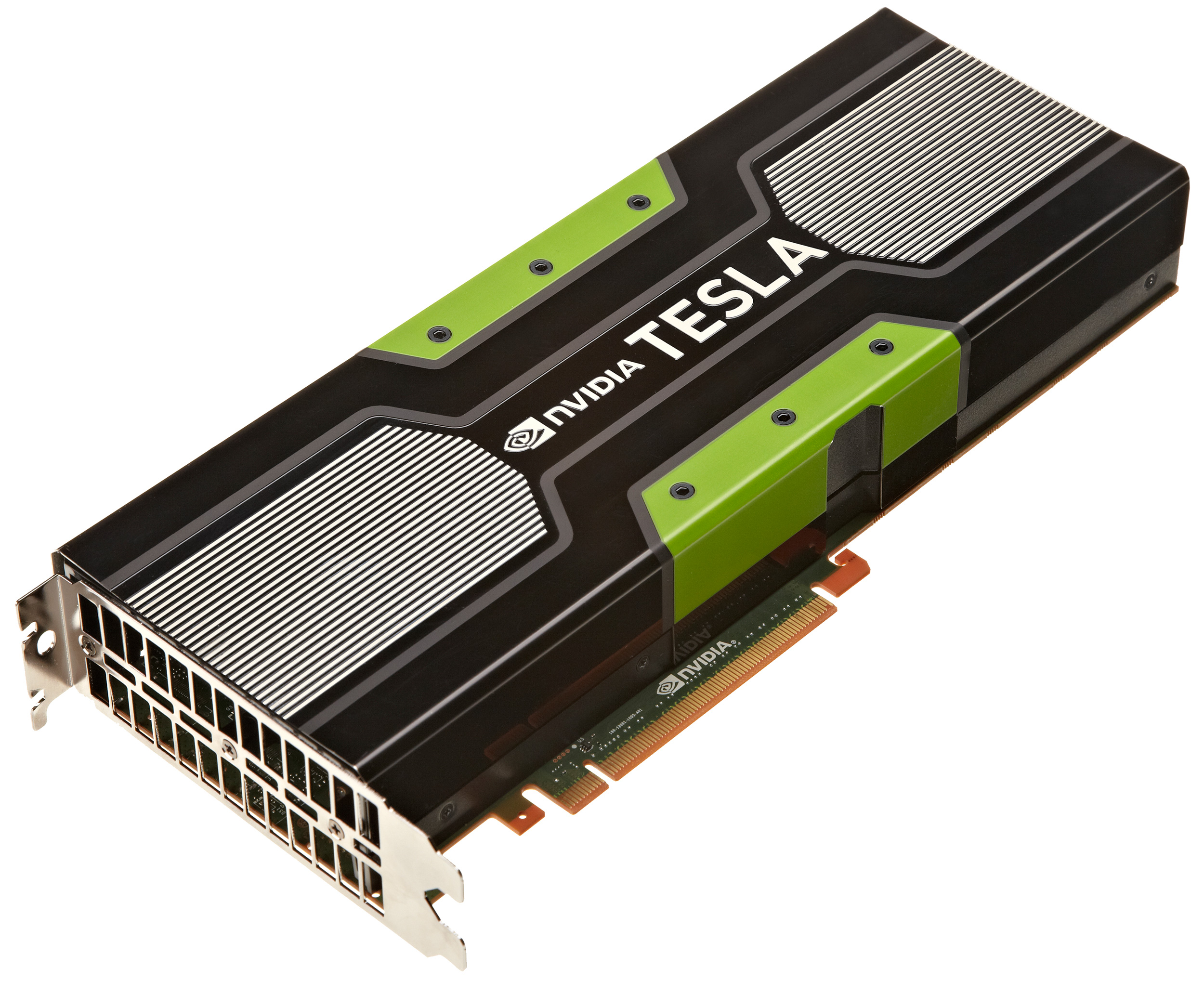
NVIDIA Launches Tesla K20 & K20X: GK110 Arrives At Last
by Ryan Smith on November 12, 2012 9:00 AM ESTContinuing our SC12 related coverage today, while AMD was the first GPU announcement of the day they are not the only one. NVIDIA is also using the venue to launch their major GPU compute product for the year: Tesla K20.
We first saw Tesla K20 at NVIDIA’s 2012 GPU Technology Conference, where NVIDIA first announced the K20 along with the already shipping K10. At the time NVIDIA was still bringing up the GPU behind K20 – GK110 – with the early announcement at GTC offering an early look at the functionality it would offer in order to prime the pump for developers. At the time we knew quite a bit about its functionality, but not its pricing, configuration, or performance.
More recently, upon completion of K20 NVIDIA has dedicated most of the initial allocation to Oak Ridge National Laboratory’s Titan supercomputer, completing delivery on a contract years in the making. As it turned out K20 was quite powerful indeed, and with K20 providing some 90% of the computational throughput of the supercomputer, Titan has taken the #1 spot on the fall Top500 supercomputer list.
This brings us to today. With Titan complete NVIDIA can now focus their attention and their GPU allocations towards making the Tesla K20 family available to the public at large. With SC12 and the announcement of the new Top500 list as their backdrop, today NVIDIA will be officially launching the Tesla K20 family of compute GPUs.
| NVIDIA Tesla Family Specification Comparison | ||||||
| Tesla K20X | Tesla K20 | Tesla M2090 | Tesla M2070Q | |||
| Stream Processors | 2688 | 2496 | 512 | 448 | ||
| Core Clock | 732MHz | 706MHz | 650MHz | 575MHz | ||
| Shader Clock | N/A | N/A | 1300MHz | 1150MHz | ||
| Memory Clock | 5.2GHz GDDR5 | 5.2GHz GDDR5 | 3.7GHz GDDR5 | 3.13GHz GDDR5 | ||
| Memory Bus Width | 384-bit | 320-bit | 384-bit | 384-bit | ||
| VRAM | 6GB | 5GB | 6GB | 6GB | ||
| Single Precision | 3.95 TFLOPS | 3.52 TFLOPS | 1.33 TFLOPS | 1.03 TFLOPS | ||
| Double Precision | 1.31 TFLOPS (1/3) | 1.17 TFLOPS (1/3) | 655 GFLOPS (1/2) | 515 GFLOPS (1/2) | ||
| Transistor Count | 7.1B | 7.1B | 3B | 3B | ||
| TDP | 235W | 225W | 250W | 225W | ||
| Manufacturing Process | TSMC 28nm | TSMC 28nm | TSMC 40nm | TSMC 40nm | ||
| Architecture | Kepler | Kepler | Fermi | Fermi | ||
| Launch Price | >$3199 | $3199? | N/A | N/A | ||
When NVIDIA first announced K20 back in May we were given a number of details about the GK110 GPU that would power it, but because they were still in the process of bringing up the final silicon for GK110 we knew little about the shipping configuration for K20. What we could say for sure is that GK110 was being built with 15 SMXes, 6 memory controllers, 1.5MB of L2 cache, and that it would offer double precision (FP64) performance that was 1/3rd its single precision (FP32 rate). Now with the launch of the K20 we finally have details on what the shipping configurations will be for K20.
First and foremost, K20 will not be a single GPU but rather it will be a family of GPUs. NVIDIA has split up what was previously announced as a single GPU into two GPUs: K20 and K20X. K20X is the more powerful of these GPUs, featuring 14 active SMXes along with all 6 memory controllers and 1.5MB of L2 cache, attached to 6GB of GDDR5. It will be clocked at 732MHz for the core clock and 5.2GHz for the memory clock. This sets a very high bar for theoretical performance, with FP32 performance at 3.95 TFLOPS, FP64 performance at 1.31 TFLOPS, and fed by some 250GB/sec of memory bandwidth. For those of you who have kept an eye on Titan, these are the same specs as the GPUs Titan, and though NVIDIA would not name it at the time we can now confirm that Titan is in fact composed of K20X GPUs and not K20.
Below K20X will be the regular K20. K20 gives up 1 SMX and 1 memory controller, giving it 13 SMXes, 5 memory controllers, 1.25MB of L2 cache, and 5GB of GDDR5. It will also be clocked slightly lower than K20X, with a shipping core clock of 706MHz while the memory clock is held at 5.2GHz. This will give K20 theoretical performance numbers around 3.52 TFLOPS for FP32, 1.17 TFLOPS for FP64, fed by 208GB/sec of memory bandwidth.
This split ends up being very similar to what NVIDIA eventually did with the Fermi generation of Tesla products such as the M2090 and M2075, spacing their products not only by performance and pricing, but also by power consumption. K20X will be NVIDIA’s leading Tesla K20 product, offering the best performance at the highest power consumption (235W). K20 meanwhile will be cheaper, a bit slower, and perhaps most importantly lower power at 225W. On that note, despite the fact that the difference is all of 10W, 225W is a very important cutoff in the HPC space – many servers and chasses are designed around that being their maximum TDP for PCIe cards – so it was important for NVIDIA to offer as fast a card as possible at this TDP, alongside the more powerful but more power hungry K20X. This tiered approach also enables the usual binning tricks, allowing NVIDIA to do something with chips that won’t hit the mark for K20X.
Moving on, at the moment NVIDIA is showing off the passively cooled K20 family design, confirming in the process that both K20 and K20X can be passively cooled as is the standard for servers. NVIDIA’s initial wave of focus for the Telsa K20 is going to be on servers (it is SC12 after all), but with K20 also being an integral part of NVIDIA’s next-generation Maximus strategy we’re sure to see actively cooled workstation models soon enough.


73 Comments
View All Comments
CeriseCogburn - Thursday, November 29, 2012 - link
LOL - wrong again amd fanboyBullwinkle J Moose - Tuesday, November 13, 2012 - link
K20X384 bit bus
6 GB VRAM
7.1 Billion Transistors
3.95 TFLOP Single Precision
1.31 TFLOP Double Precision
$3200
Sounds impressive but can it play Crisis?
Bullwinkle J Moose - Wednesday, November 14, 2012 - link
CRYSISCeriseCogburn - Thursday, November 29, 2012 - link
You both meant Crysis Warhead, frost bench, an amd advantage favorite for a single amd win of late, not Crysis 2.LOL
the bias is screaming out
eddman - Monday, November 12, 2012 - link
"I am a Nvidia fanboi."You do know that fanboy means "A stupid and highly biased fan", right?
The term you'd want to use is simply "Fan".
Denithor - Monday, November 12, 2012 - link
I think that was his point exactly - he's a RABID nVidia fan but still finds it off balance the differential treatment for the two companies.CeriseCogburn - Thursday, November 29, 2012 - link
The truth is probably he's a rabid amd fanboy in disguiseSabresiberian - Tuesday, November 13, 2012 - link
The "stupid" part is YOUR interpretation, it's not what it means to most people.Biased, yes, stupid, no.
CeriseCogburn - Thursday, November 29, 2012 - link
Biased because, while being so stupid, so obsessed, so doused in tampon and motrin lacking estrogenic emoting for the team, that facts simply do not matter, and spinning Barney and and Nancy and Harry would be proud of, becomes all that spews forth.Stupid is definitely part of it, coupled with a huge liar factor.
It may be the washing of the brain coupled with the excessive female hormone problems are the base cause, but in every case except flat out devious lying troll for amd, paid or unpaid, stupidity is a very large component.
dragonsqrrl - Monday, November 12, 2012 - link
'An article about an AMD product got only 1 page of coverage while an article about an Nvidia product got 3, BIAS, FAVORITISM, FANBOI'Dude really, grow up. You're just about the last person who should be throwing around accusations of bias and fanboism. Do you really have nothing better to do than to troll and whine on Tom's and Anand, about how the whole world is conspiring against your benevolent AMD?