The Tegra 4 GPU, NVIDIA Claims Better Performance Than iPad 4
by Anand Lal Shimpi on January 14, 2013 6:13 PM ESTAt CES last week, NVIDIA announced its Tegra 4 SoC featuring four ARM Cortex A15s running at up to 1.9GHz and a fifth Cortex A15 running at between 700 - 800MHz for lighter workloads. Although much of CEO Jen-Hsun Huang's presentation focused on the improvements in CPU and camera performance, GPU performance should see a significant boost over Tegra 3.
The big disappointment for many was that NVIDIA maintained the non-unified architecture of Tegra 3, and won't fully support OpenGL ES 3.0 with the T4's GPU. NVIDIA claims the architecture is better suited for the type of content that will be available on devices during the Tegra 4's reign.
Despite the similarities to Tegra 3, components of the Tegra 4 GPU have been improved. While we're still a bit away from a good GPU deep-dive on the architecture, we do have more details than were originally announced at the press event.
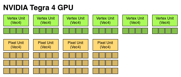
Tegra 4 features 72 GPU "cores", which are really individual components of Vec4 ALUs that can work on both scalar and vector operations. Tegra 2 featured a single Vec4 vertex shader unit (4 cores), and a single Vec4 pixel shader unit (4 cores). Tegra 3 doubled up on the pixel shader units (4 + 8 cores). Tegra 4 features six Vec4 vertex units (FP32, 24 cores) and four 3-deep Vec4 pixel units (FP20, 48 cores). The result is 6x the number of ALUs as Tegra 3, all running at a max clock speed that's higher than the 520MHz NVIDIA ran the T3 GPU at. NVIDIA did hint that the pixel shader design was somehow more efficient than what was used in Tegra 3.
If we assume a 520MHz max frequency (where Tegra 3 topped out), a fully featured Tegra 4 GPU can offer more theoretical compute than the PowerVR SGX 554MP4 in Apple's A6X. The advantage comes as a result of a higher clock speed rather than larger die area. This won't necessarily translate into better performance, particularly given Tegra 4's non-unified architecture. NVIDIA claims that at final clocks, it will be faster than the A6X both in 3D games and in GLBenchmark. The leaked GLBenchmark results are apparently from a much older silicon revision running no where near final GPU clocks.
| Mobile SoC GPU Comparison | |||||||||||||||
| GeForce ULP (2012) | PowerVR SGX 543MP2 | PowerVR SGX 543MP4 | PowerVR SGX 544MP3 | PowerVR SGX 554MP4 | GeForce ULP (2013) | ||||||||||
| Used In | Tegra 3 | A5 | A5X | Exynos 5 Octa | A6X | Tegra 4 | |||||||||
| SIMD Name | core | USSE2 | USSE2 | USSE2 | USSE2 | core | |||||||||
| # of SIMDs | 3 | 8 | 16 | 12 | 32 | 18 | |||||||||
| MADs per SIMD | 4 | 4 | 4 | 4 | 4 | 4 | |||||||||
| Total MADs | 12 | 32 | 64 | 48 | 128 | 72 | |||||||||
| GFLOPS @ Shipping Frequency | 12.4 GFLOPS | 16.0 GFLOPS | 32.0 GFLOPS | 51.1 GFLOPS | 71.6 GFLOPS | 74.8 GFLOPS | |||||||||
Tegra 4 does offer some additional enhancements over Tegra 3 in the GPU department. Real multisampling AA is finally supported as well as frame buffer compression (color and z). There's now support for 24-bit z and stencil (up from 16 bits per pixel). Max texture resolution is now 4K x 4K, up from 2K x 2K in Tegra 3. Percentage-closer filtering is supported for shadows. Finally, FP16 filter and blend is supported in hardware. ASTC isn't supported.
If you're missing details on Tegra 4's CPU, be sure to check out our initial coverage.


59 Comments
View All Comments
CeriseCogburn - Sunday, January 20, 2013 - link
What happened with AMD then ? They had the same advantages as Apple, and all we ever heard was they were a huge financial burden that was not AMD fault whatsoever...
AMD took a different strategy compared to Apple - smaller/cheaper/crashier....
Thus it has nearly destroyed them.
So one can talk advantages all the time, but those with a very similar set often evolve quite differently, one to wild success and a truly dedicated deep pocketed following(appleheads) willing to provide profits and guard their precious IOS babies for years on end, and another teetering on bankruptcy and constant humiliation and penny pinching with a tightwad fanatic user fan base always trying to the very last drop of red AMD blood from the rotten turnip while attacking and blaming everyone else in a now failed PR war that has been **** on the industry for years.
nVidia on the other hand was pushed out of the chipset business and instead of publicly making a big sick stinking hate bomb over it and training their fanboys to take up the cause like AMD would have, they continued to excel in their other base nVidia #1 business while they branched out and aimed for the future - pulling in a fine profit and remaining a top dog.
Project Shield has impressed those who used it hands on, so we already know the tegra4 is a coming winner.
Just click the tegra2 tegra3 and tegra4 buttons in the build graph there and "astounding!" sounds correct for the architectural size differences.
If one is concerned about power as a few mentioned, that fifth core is the "idler" that is going to make this chip tremendous in power saving features.
I want one yesterday.
EnzoFX - Monday, January 14, 2013 - link
Exactly, let alone the advantages Apple has with vertical integration i.e. optimized performance.ltcommanderdata - Monday, January 14, 2013 - link
Besides shader ALUs are there any details on changes to TMU and ROP count? Are those also scaled 6x or only 2x corresponding to the doubling of Vec4 pixel units rather than the ALUs themselves?As well, for you chart, could you add a row stating the "shipping clocks" you are using to calculate your GFLOPS results since that makes things more clear.
Brunelleschi - Monday, January 14, 2013 - link
Tegra 4 sounds really awesome!! I wish a unified shader architecture were used, but still, if the shipping frequencies are 600MHz or above, the Tegra 4 should be significantly ahead of the A6X, despite the non-unified shader architecture. I think this will be because, even with Tegra 3's non-unified shader architecture, which could only do 12 GFLOPS in total, it wasn't much behind the PowerVR SGX543MP2 in the iPad 2 (with 16 GFLOPS total).I think that the Tegra 4 will be pretty revolutionary for mobile GPU performance, especially in the Android world, because nor the Mali-T604 nor the PowerVR SGX544MP3 in the Exynos 5 Octa stand a chance against the Tegra 4, even with the older architecture. I only wished NVIDIA used a Mobile Development Platform, like Qualcomm does, so we wouldn't have to wait for an actual device to be released to the market to see the SoC's performance. (If only NVIDIA let people try the SHIELD sample device at CES...)
KitsuneKnight - Monday, January 14, 2013 - link
Tegra 4 will increase performance over last gen parts, but it'll still lack full OpenGL ES 3.0 support. Current gen Mali and Adreno GPUs already support OpenGL ES 3.0, and PowerVR GPUs will begin supporting it with Rogue. That's going to suck for game developers, having one major vendor not support the standard, which means it'll be even longer before a high enough percentage of the market can handle OGLES3.0 that developers are comfortable requiring it, instead of spending extra time, effort, and money to write extra code paths.If nVidia can get the Tegra 4 out before the next iPad, it'll likely be top tier for a bit... but if they're too slow, newer GPUs will enter the market from all the other vendors (including the first PowerVR Series 6 GPUs) which'll make Tegra 4 look like nothing special, and maybe even look anemic in comparison. So far, nVidia's mobile hype hasn't lived up to their marketing... hopefully the Tegra 4's GPU will be nothing like their older GPUs.
DERSS - Tuesday, January 15, 2013 - link
A7X will probably debut before actual Tegra 4 devices will ship, though.CeriseCogburn - Sunday, January 20, 2013 - link
So as per Apple's terse standard method pointed out here, you're saying A7X in retail apple devices will hit the markets less than 10 days after the 1st tegra4 devices...LOL
Whatever... more bloviation from the superspeculator with zero facts and zero history on their side.
A snide smear is not the future applefan or nVidia hater.
tviceman - Monday, January 14, 2013 - link
Since Nvidia's dull CES event, horrible Tegra 4 intro, perplexing decision to create SHIELD, and the leaked benchmarks, I've been really down on Tegra 4. If this news is true, then I'll probably change my mind. Nvidia cannot afford to come out with a chip slower than what the competition has had out for 3, 6, even 9 months already.Being on 28nm and using TSMC's lowest leakage process, perf/watt should be considerably better than Samsung's exynos 5. I've also come to the conclusion that SHIELD is using Tegra 4 chips that will end up not making the cut for tablets and phones with respect to clockspeeds / voltages / TDP for to essentially maximize the amount of money they can squeeze out of each Tegra 4 wafer.
joos2000 - Monday, January 14, 2013 - link
I would like to see an added row showing GFLOPS/Watt.Ryan Smith - Monday, January 14, 2013 - link
GFLOPS/watt varies non-linearly with clockspeed, so it would be extremely product specific at best.