NVIDIA’s GeForce GTX Titan Review, Part 2: Titan's Performance Unveiled
by Ryan Smith & Rahul Garg on February 21, 2013 9:00 AM ESTThe Final Word On Overclocking
Before we jump into our performance breakdown, I wanted to take a few minutes to write a bit of a feature follow-up to our overclocking coverage from Tuesday. Since we couldn’t reveal performance numbers at the time – and quite honestly we hadn’t even finished evaluating Titan – we couldn’t give you the complete story on Titan. So some clarification is in order.
On Tuesday we discussed how Titan reintroduces overvolting for NVIDIA products, but now with additional details from NVIDIA along with our own performance data we have the complete picture, and overclockers will want to pay close attention. NVIDIA may be reintroducing overvolting, but it may not be quite what many of us were first thinking.
First and foremost, Titan still has a hard TDP limit, just like GTX 680 cards. Titan cannot and will not cross this limit, as it’s built into the firmware of the card and essentially enforced by NVIDIA through their agreements with their partners. This TDP limit is 106% of Titan’s base TDP of 250W, or 265W. No matter what you throw at Titan or how you cool it, it will not let itself pull more than 265W sustained.
Compared to the GTX 680 this is both good news and bad news. The good news is that with NVIDIA having done away with the pesky concept of target power versus TDP, the entire process is much simpler; the power target will tell you exactly what the card will pull up to on a percentage basis, with no need to know about their separate power targets or their importance. Furthermore with the ability to focus just on just TDP, NVIDIA didn’t set their power limits on Titan nearly as conservatively as they did on GTX 680.
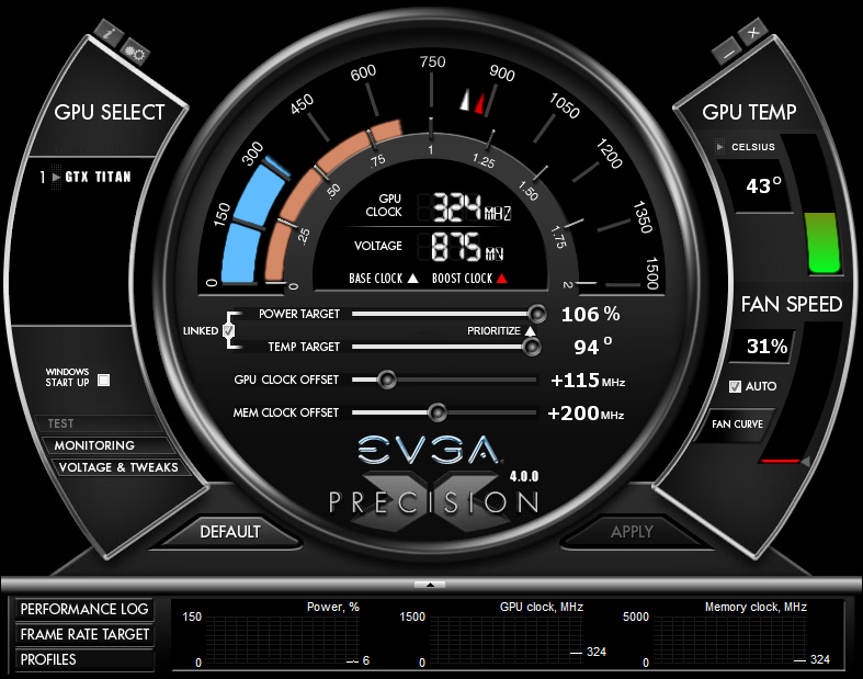
The bad news is that while GTX 680 shipped with a max power target of 132%, Titan is again only 106%. Once you do hit that TDP limit you only have 6% (15W) more to go, and that’s it. Titan essentially has more headroom out of the box, but it will have less headroom for making adjustments. So hardcore overclockers dreaming of slamming 400W through Titan will come away disappointed, though it goes without saying that Titan’s power delivery system was never designed for that in the first place. All indications are that NVIDIA built Titan’s power delivery system for around 265W, and that’s exactly what buyers will get.
Second, let’s talk about overvolting. What we didn’t realize on Tuesday but realize now is that overvolting as implemented in Titan is not overvolting in the traditional sense, and practically speaking I doubt too many hardcore overclockers will even recognize it as overvolting. What we mean by this is that overvolting was not implemented as a direct control system as it was on past generation cards, or even the NVIDIA-nixed cards like the MSI Lightning or EVGA Classified.
Overvolting is instead a set of two additional turbo clock bins, above and beyond Titan’s default top bin. On our sample the top bin is 1.1625v, which corresponds to a 992MHz core clock. Overvolting Titan to 1.2 means unlocking two more bins: 1006MHz @ 1.175v, and 1019MHz @ 1.2v. Or put another way, overvolting on Titan involves unlocking only another 27MHz in performance.
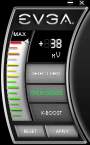
These two bins are in the strictest sense overvolting – NVIDIA doesn’t believe voltages over 1.1625v on Titan will meet their longevity standards, so using them is still very much going to reduce the lifespan of a Titan card – but it’s probably not the kind of direct control overvolting hardcore overclockers were expecting. The end result is that with Titan there’s simply no option to slap on another 0.05v – 0.1v in order to squeak out another 100MHz or so. You can trade longevity for the potential to get another 27MHz, but that’s it.
Ultimately, this means that overvolting as implemented on Titan cannot be used to improve the clockspeeds attainable through the use of the offset clock functionality NVIDIA provides. In the case of our sample it peters out after +115MHz offset without overvolting, and it peters out after +115MHz offset with overvolting. The only difference is that we gain access to a further 27MHz when we have the thermal and power headroom available to hit the necessary bins.
| GeForce GTX Titan Clockspeed Bins | |||
| Clockspeed | Voltage | ||
| 1019MHz | 1.2v | ||
| 1006MHz | 1.175v | ||
| 992MHz | 1.1625v | ||
| 979MHz | 1.15v | ||
| 966MHz | 1.137v | ||
| 953MHz | 1.125v | ||
| 940MHz | 1.112v | ||
| 927MHz | 1.1v | ||
| 914MHz | 1.087v | ||
| 901MHz | 1.075v | ||
| 888MHz | 1.062v | ||
| 875MHz | 1.05v | ||
| 862MHz | 1.037v | ||
| 849MHz | 1.025v | ||
| 836MHz | 1.012v | ||
Finally, as with the GTX 680 and GTX 690, NVIDIA will be keeping tight control over what Asus, EVGA, and their other partners release. Those partners will have the option to release Titan cards with factory overclocks and Titan cards with different coolers (i.e. water blocks), but they won’t be able to expose direct voltage control or ship parts with higher voltages. Nor for that matter will they be able to create Titan cards with significantly different designs (i.e. more VRM phases); every Titan card will be a variant on the reference design.
This is essentially no different than how the GTX 690 was handled, but I think it’s something that’s important to note before anyone with dreams of big overclocks throws down $999 on a Titan card. To be clear, GPU Boost 2.0 is a significant improvement in the entire power/thermal management process compared to GPU Boost 1.0, and this kind of control means that no one needs to be concerned with blowing up their video card (accidentally or otherwise), but it’s a system that comes with gains and losses. So overclockers will want to pay close attention to what they’re getting into with GPU Boost 2.0 and Titan, and what they can and cannot do with the card.


337 Comments
View All Comments
PEJUman - Thursday, February 21, 2013 - link
Made me wonder:7970 - 4.3B trans. - $500 - OK compute, 100% gaming perf.
680 - 3.5B trans. _ $500 - sucky compute, 100% gaming perf.
Titan - 7.1B trans - $1000 - OK compute, ~140% gaming perf.
1. Does compute capability really takes that much more transistors to build? as in 2x trans. only yield ~140% improvement on gaming.
I think this was a conscious decision by nVidia to focus on compute and the required profit margin to sustain R&D.
2. despite the die size shrink, I'm guessing it would be harder to have functional silicon as the process shrinks. i.e. finding 100mm^2 of functional silicon @ 40nm is easier than @28nm, from the standpoint that more transistors are packed to the same area. Which I think why they have 15SMXs designed.
Thus it'd be more expensive for nVidia to build same area at 28 vs. 40 nm... at least until the process matures, but at 7B I doubt it will ever be attainable.
3. The AMD statement on no updates to 7970 essentially sealed the $1000 price for titan. I would bet if AMD announced 8970, Titan would be priced at $700 today, with 3GB memory.
JarredWalton - Thursday, February 21, 2013 - link
Luxury GPU is no more silly than Extreme CPUs that cost $1000 each. And yet, Intel continues to sell those, and what's more the performance offered by Titan is a far better deal than the performance offered by a $1000 CPU vs. a $500 CPU. Then there's the Tesla argument: it's a $3500 card for the K20 and this is less than a third that price, with the only drawbacks being no ECC and no scalability beyond three cards. For the Quadro crowd, this might be a bargain at $1000 (though I suspect Titan won't get the enhanced Quadro drivers, so it's mostly a compute Tesla alternative).chizow - Friday, February 22, 2013 - link
The problem with this analogy, which I'm sure was floated around Nvidia's Marketing board room in formulating the plan for Titan, is that Intel offers viable alternative SKUs based on the same ASIC. Sure there are the few who will buy the Intel EE CPU (3970K) for $1K, but the overwhelming majority in that high-end market would rather opt for the $500 option (3930K) or $300 option (3820).Extend this to the GPU market and you see Nvidia clearly withheld GK100/GK110 as the flagship part for over a year, and instead of offering a viable SKU for traditional high-end market segments based on this ASIC, they created a NEW ultra-premium market. That's the ONLY reason Titan looks better compared to GK104 than Intel's $1K and $500 options, because Nvidia's offerings are truly different classes while Intel's differences are minor binning and multiplier locked parts with a bigger black box.
mlambert890 - Saturday, February 23, 2013 - link
The analogy is fine, you're just choosing to not see it.Everything you said about Intel EE vs standard directly applies here.
You are assuming that the Intel EE parts are nothing more than a marketing ploy, which is wrong, while at the same time assuming that the Titan is orders of magnitude beyond the 680 which is also wrong.
You're seeing it from the point of view of someone who buys the cheapest Intel CPU, overclocks it to the point of melting, and then feels they have a solution "just as good if not better" than the Intel EE.
Because the Titan has unlocked stream procs that the 680 lacks, and there is no way to "overclock" your way around missing SPs, you feel that NVidia has committed some great sin.
The reality is that the EE procs give out of box performance that is superior to out of box performance of the lesser SKUs by a small, but appreciable, margin. In addition, they are unlocked, and come from a better bin, which means they will overclock *even better* than the lesser SKUs. Budget buyers never want to admit this, but it is reality in most cases. Yes you can get a "lucky part" from the lesser SKU that achieves a 100% overclock, but this is an anomaly. Most who criticize the EE SKUs have never even come close to owning one.
Similarly, the Titan offers a small, but appreciable, margin of performance over the 680. It allows you to wait longer before going SLI. The only difference is you don't get the "roll of the dice" shot at a 680 that *might* be able to appear to match a Titan since the SP's arent there.
The analogy is fine, it's just that biased perspective prevents some from seeing it.
chizow - Saturday, February 23, 2013 - link
Well you obviously have trouble comprehending analogies if you think 3.6B difference in transistors and ~40% difference in performance is analogous to 3MB L3 cache, an unlocked multiplier and 5% difference in performance.But I guess that's the only way you could draw such an asinine parallel as this:
"Similarly, the Titan offers a small, but appreciable, margin of performance over the 680."
It's the only way your ridiculous analogy to Intel's EE could possibly hold true, when in reality, it couldn't be further from the truth. Titan holds a huge advantage over GTX 680, but that's expected, its a completely different class of GPU whereas the 3930K and 3960X are cut from the exact same wafer.
CeriseCogburn - Sunday, February 24, 2013 - link
There was no manufacturing capacity you IDIOT LIAR.The 680 came out 6 months late, and amd BARELY had 79xx's on the shelves till a day before that.
Articles were everywhere pointing out nVidia did not have reserve die space as the crunch was extreme, and the ONLY factory was in the process of doing a multi-billion dollar build out to try to keep up with bare minimum demand.
Now we've got a giant GPU core with perhaps 100 attempted dies per wafer, with a not high yield, YET YOU'RE A LIAR NONETHELESS.
chizow - Sunday, February 24, 2013 - link
It has nothing to do with manufacturing capacity, it had everything to do with 7970's lackluster performance and high price tag.GTX 680 was only late (by 3, not 6 months) because Nvidia was too busy re-formulating their high-end strategy after seeing 7970 outperform GTX 580 by only 15-20% but asking 10% higher price. Horrible price:performance metric for a new generation GPU on a new process node.
This gave Nvidia the opportunity to:
1) Position mid-range ASIC GK104 as flagship GTX 680 and still beat the 7970.
2) Push back and most importantly, re-spin GK100 and refine it to be GK110.
3) Screw their long-time customers and AMD/AMD fans in the process.
4) Profit.
So instead of launching and mass-producing their flagship ASIC first (GK100) as they've done in every single previous generation and product launch, they shifted their production allocation at TSMC to their mid-range ASIC, GK104 instead.
Once GK110 was ready, they've had no problem churning them out, even the mfg date of these TITAN prove this point as week 31 chips are somewhere in the July-August time frame. They were able to deliver some 19,000 K20X units to ORNL for the real TITAN in October 2012. Coupled with the fact they're using ASICs with the same number of functional units for GTX Titanic, it goes to show yields are pretty good.
But the real conclusion to be drawn for this is that other SKUs based on GK110 are coming. There's no way GK110 wafer yields are anywhere close to 100% for 15 SMX ASICs. I fully expect a reduced SMX unit, maybe 13 with 2304SP as originally rumored show it's face as the GTX 780 with a bunch of GK114 refreshes behind it to fill out the line-up.
The sooner people stop overpaying for TITAN, the sooner we'll see the GTX 700 series, imo, but with no new AMD GPUs on the horizon we may be waiting awhile.
CeriseCogburn - Sunday, February 24, 2013 - link
Chizow I didn't read your stupid long post except for your stupid 1st line.you're a brainwashed lying sack of idiocy, so maybe i'll waste my time reading your idiotic lies, and maybe not, since your first line is the big fat frikkin LIE you HAVE TO BELIEVE that you made up in your frikkin head, in order to take your absolutely FALSE STANCE for the past frikkin nearly year now.
chizow - Monday, February 25, 2013 - link
You should read it, you might learn something.Until then stfd, stfu, and gfy.
CeriseCogburn - Sunday, February 24, 2013 - link
Dear Jeff, a GPU that costs $400 dollars is a luxury GPU.I'm not certain you disagree with that, I'd just like to point out the brainless idiots pretending $1000 for a GPU is luxury and $250 is not are clueless.