Intel's Return to DRAM: Haswell GT3e to Integrate 128MB eDRAM?
by Anand Lal Shimpi on April 23, 2013 11:58 AM EST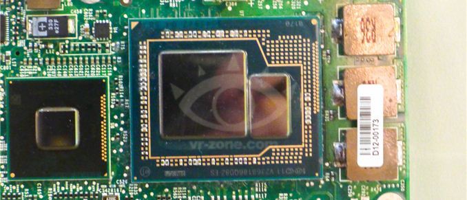
We've known for a while now that Intel will integrate some form of DRAM on-package for the absolute highest end GPU configurations of its upcoming Haswell SoC. Memory bandwidth is a very important enabler of GPU (and multi-core CPU) performance, but delivering enough of it typically required very high speed interfaces (read: high power) and/or very wide interfaces (read: large die areas). Neither of the traditional approaches to scaling memory bandwidth are low power or cost effective, which have kept them out of ultra mobile and integrated processor graphics.
The days of simple performance scaling by throwing more transistors at a design are quickly coming to an end. Moore's Law will continue but much like the reality check building low power silicon gave us a while ago, building high performance silicon will need some out of the box thinking going forward.
Dating back to Ivy Bridge (3rd gen Core/2012), Intel had plans to integrate some amount of DRAM onto the package in order to drive the performance of its processor graphics. Embedding DRAM onto the package adds cost and heat, and allegedly Paul Otellini wasn't willing to greenlight the production of a part that only Apple would use so it was canned. With Haswell, DRAM is back on the menu and this time it's actually going to come out. We've referred to the Haswell part with embedded DRAM as Haswell GT3e. The GT3 refers to the GPU configuration (40 EUs), while the lowercase e denotes embedded DRAM. Haswell GT3e will only be available in a BGA package (soldered-on, not socketed), and is only expected to appear alongside higher TDP (read: not Ultrabook) parts. The embedded DRAM will increase the thermal load of the SoC, although it shouldn't be as painful as including a discrete GPU + high speed DRAM. Intel's performance target for Haswell GT3e is NVIDIA's GeForce GT 650M.
What we don't know about GT3e is the type, size and speed of memory that Intel will integrate. Our old friend David Kanter at RealWorldTech presented a good thesis on the answers to those questions. Based on some sound logic and digging through the list of papers to be presented at the 2013 VLSI Technology Symposium in Kyoto, Kanter believes that the title of this soon to be presented Intel paper tells us everything we need to know:
"A 22nm High Performance Embedded DRAM SoC Technology Featuring Tri-Gate Transistors and MIMCAP COB"
According to Kanter's deductions (and somewhat validated by our own sources), Haswell GT3e should come equipped with 128MB of eDRAM connected to the main SoC via a 512-bit bus. Using eDRAM vs. commodity DDR3 makes sense as the former is easier to integrate into Intel's current fabs. There are also power, manufacturability and cost concerns as well that resulted in the creation of Intel's own DRAM design. The interface width is a bit suspect as that would require a fair amount of area at the edges of the Haswell die, but the main takeaway is that we're dealing with a parallel interface. Kanter estimates the bandwidth at roughly 64GB/s, not anywhere near high-end dGPU class but in the realm of what you can expect from a performance mainstream mobile GPU. At 22nm, Intel's eDRAM achieves a density of around 17.5Mbit/mm^2, which works out to be ~60mm^2 for the eDRAM itself. Add in any additional interface logic and Kanter estimates the total die area for the eDRAM component to be around 70 - 80mm^2. Intel is rumored to be charging $50 for the eDRAM adder on top of GT3, which would deliver very good margins for Intel. It's a sneaky play that allows Intel to capture more of the total system BoM (Bill of Materials) that would normally go to a discrete GPU company like NVIDIA, all while increasing utilization of their fabs. NVIDIA will still likely offer better perfoming solutions, not to mention the benefits of much stronger developer relations and a longer history of driver optimization. This is just the beginning however.
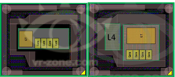
Based on leaked documents, the embedded DRAM will act as a 4th level cache and should work to improve both CPU and GPU performance. In server environments, I can see embedded DRAM acting as a real boon to multi-core performance. The obvious fit in the client space is to improve GPU performance in games. At only 128MB I wouldn't expect high-end dGPU levels of performance, but we should see a substantial improvement compared to traditional processor graphics. Long term you can expect Intel to bring eDRAM into other designs. There's an obvious fit with its mobile SoCs, although there we're likely talking about something another 12 - 24 months out.
AMD is expected to integrate a GDDR5 memory controller in its future APUs, similar to what it has done with the PlayStation 4 SoC, as its attempt to solve the memory bandwidth problem for processor based graphics.
Source: RealWorldTech


83 Comments
View All Comments
Kevin G - Tuesday, April 23, 2013 - link
To address the first idea, IBM does use eDRAM in their high end POWER line and their System Z mainframes. The POWER7+ has 80 MB of eDRAM on-die. The mainframes are even beefier with 48 MB of eDRAM L3 cache on die and a massive 384 MB external L4. Those systems are not x86 based but they are fast. Intel going with eDRAM would likely perform similarly. However, it should be noted that Intel has focused on latencies with their caches, not capacities.Having a common cache between the integrated CPU and GPU would be advantageous for the very reasons you cite. While it didn't get a lot of press, Intel does have a unified address space between their HD graphics in Sandybridge/Ivy Bridge. So essentially Haswell GT3e will have the functionality.
With regards to Xeon + discrete GPU though, there will always be overhead by merit of PCI-e connectivity even if the GPU is using the same x86 address space. It'll be higher bandwidth and lower latency than today but the results will be nothing like the on-die integration we're seeing on the consumer side. Just having everything on-die helps a lot. Then again, both AMD and Intel can remove PCI-e and ship discrete GPU's using their own proprietary processor interconnects (HyperTransport and QPI respectively). At this point the discrete GPU would be logically seen as another socket node.
bernstein - Tuesday, April 23, 2013 - link
that last bit of connecting a gpu via QPI/HyperTransport is a very interesting proposition. However what would be the performance gains? it's not even twice the speed of x16 pcie3, so i guess it's mostly direct memory access & latency. right?Kevin G - Tuesday, April 23, 2013 - link
For the most part, yes, lower latency and direct memory access as if they were another socket/core. This idea isn't new either. One of Intel's early slide decks regarding Larrabee had mention of a Larrabee chip that'd drop into a quad socket motherboard.I'm actually quiet surprised that AMD hasn't gone this route or have many any mention of it on their road maps. They do have new sockets coming out next year and HSA GPU's so perhaps next year we'll hear something a bit more concrete.
The other thing about using a common socket between a CPU and a GPU would be that each aspect would have to support a common memory standard. AMD looks to be going with GDDR5 for mobile parts for bandwidth reasons. Considering that laptops (and especially ultra books) are not designed for upgradability or 24/7 rock hard stability. It also means that more desktop/server centric sockets would imply support for ECC protected DIMMs. This would also bring huge amounts of memory support to the GPU side. These two things would be huge on the GPU side.
One thing moving to QPI/Hypertransport for GPU's would result in is the eventual removal of nVidia from this space. PCI-e will still hang around but hardware using it would be at a disadvantage.
Musafir_86 - Tuesday, April 23, 2013 - link
-Hmm, are SB & IB really have unified memory address space between CPU & GPU? CPU can access GPU memory pointers & vice-versa? Like AMD's upcoming Kaveri? Any documentation/white paper from Intel on this?-What I know is their L2/L3 caches are definitely shared/unified, though. Intel's Instantaccess DX extension is only implemented in Haswell, so I doubt this is the case.
Regards.
jasonelmore - Tuesday, April 23, 2013 - link
Ivy Bridge cant share L3 with CPU and GT and both use it at the same time, Haswell fix's this issue and unifies it. A lot of ppl are getting this wrong.Jaybus - Thursday, April 25, 2013 - link
Thus the focus on silicon photonics Intel, IBM, and others have been working on. Interconnects such as QPI, HyperTransport, or Xilinx's RapidIO use too much power and/or require much more space for multiple parallel i/o traces. An optical interconnect eliminates many of the restraints imposed by QPI. The optical signal frequency can be orders of magnitude higher than what is possible for electronic signals without increasing power or thermal load. It is not possible, long term, to continue to integrate components onto a single larger and larger piece of silicon (ie. SoC).Silicon photonics is a way to connect chip-to-chip at full chip speed, or in other words connect multiple chips together to make a single large virtual chip. Since the optical signal can also maintain this high speed for far further trace distances, it can also be used to make chip-to-chip interconnects even when the chips are on different motherboards in separate cluster nodes. Think a rack of servers that function as a single, very large SoC.
We will first see it used for optical Thunderbird, (ie. extending PCIe bus off-chip), but probably for special purpose chip-to-chip soon after. For example, a CPU and discrete GPU + eDRAM pair in a 2-chip module connected via silicon waveguide.
extide - Tuesday, April 23, 2013 - link
There are indeed Xeon E3's with integrated GPU's.MrSpadge - Thursday, April 25, 2013 - link
For gaming and many desktop loads such a high-bandwidth low-latency L4 would also be cool.icrf - Tuesday, April 23, 2013 - link
Would the initial GT3e have that extra eDRAM available to the CPU as well, or is that more speculation on how such a feature might make its way onto a server part?I don't personally have much interest in a faster embedded GPU, but a pile of L4 available to the CPU sounds like it could make for some more interesting use cases.
Death666Angel - Tuesday, April 23, 2013 - link
2nd to last paragraph:"Based on leaked documents, the embedded DRAM will act as a 4th level cache and should work to improve both CPU and GPU performance."