New Elements to Samsung SSDs: The MEX Controller, Turbo Write and NVMe
by Ian Cutress on July 18, 2013 1:09 AM EST
As part of the SSD Summit in Korea today, Samsung gave the world media a brief glimpse into some new technologies. The initial focus on most of these will be in the Samsung 840 Evo, unveiled earlier today.
The MEX Controller
First up is the upgrade to the controller. Samsung’s naming scheme from the 830 onwards has been MCX (830), MDX (840, 840 Pro) and now the MEX with the 840 Evo. This uses the same 3-core ARM Cortex R4 base, however boosted from 300 MHz in the MDX to 400 MHz in the MEX. This 33% boost in pure speed is partly responsible for the overall increase in 4K random IOPS at QD1, which rise from 7900 in the 840 to 10000 in the 840 Evo (+27%). This is in addition to firmware updates with the new controller, and that some of the functions of the system have been ported as hardware ops rather than software ops.
TurboWrite
The most thought provoking announcement was TurboWrite. This is the high performance buffer inside the 840 Evo which contributes to the high write speed compared to the 840 (140 MB/s on 120GB drive with the 840, compared to 410 MB/s on the 840 Evo 120GB). Because writing to 3-bit MLC takes longer than 2-bit MLC or SLC, Samsung are using this high performance buffer in SLC mode. Then, when the drive is idle, it will pass the data on to the main drive NAND when performance is not an issue.
The amount of ‘high-performance buffer’ with the 840 Evo will depend on the model being used. Also, while the buffer is still technically 3-bit MLC, due to its use in SLC mode the amount of storage in the buffer decreases by a factor three. So in the 1TB version of the 840 Evo, which has 36 GB of buffer, in actual fact can accommodate 12 GB of writes in SLC mode before reverting to the main NAND. In the 1TB model however, TurboWrite has a minimal effect – it is in the 120GB model where Samsung are reporting the 3x increase in write speeds.
In the 120GB and 250GB models, they will have 9 GB of 3-bit MLC buffer, which will equate to 3 GB of writes. Beyond this level of writes (despite the 10GB/day oft quoted average), one would assume that the device reverts back to the former write speed – in this case perhaps closer to the 140 MB/s number from the 840, but the addition of firmware updates will go above this. However, without a drive to test it would be pure speculation, but will surely come up in the Q&A session later today, and we will update the more we know.
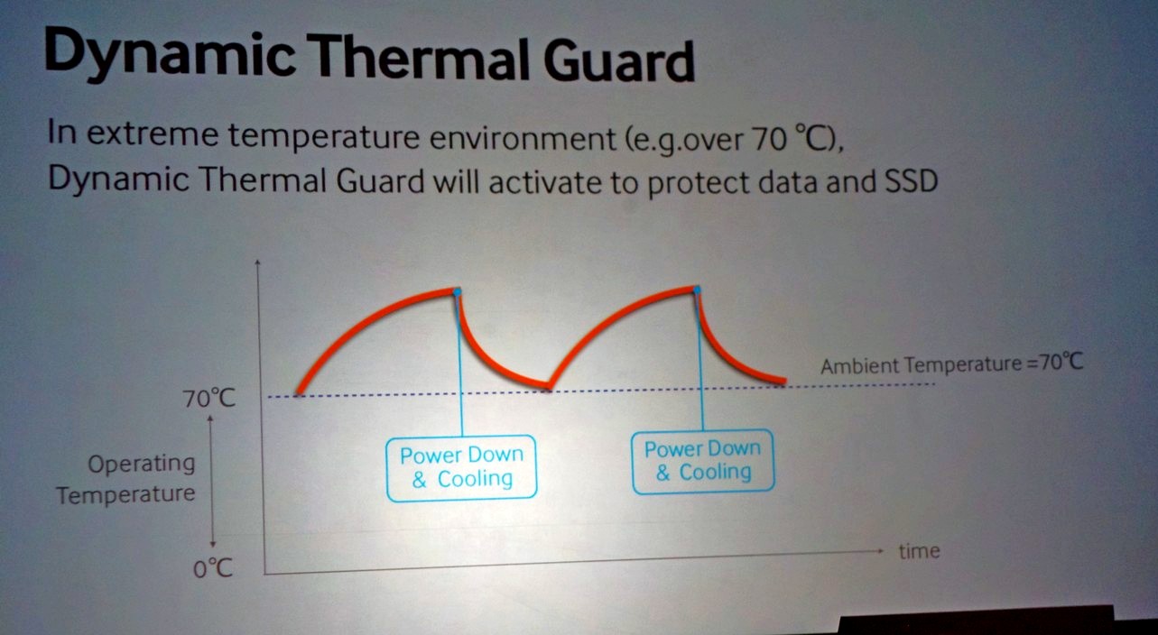
Dynamic Thermal Guard
A new feature on the 840 Evo is the addition of Dynamic Thermal Guard, where operating temperatures of the SSD are outside their suggest range (70C+). Using some programming onboard, above the predefined temperature, the drive will throttle its power usage to generate less heat until such time as the operating temperature is more normal. Unfortunately no additional details on this feature were announced, but I think this might result in a redesign for certain gaming laptops that reach 80C+ under high loading.
Non-Volatile Memory Express (NVMe)
While this is something relatively new, it is not on the 840 Evo, but as part of the summit today it is worth some discussion. The principle behind NVMe is simple – command structures like IDE and AHCI were developed with mechanical hard-disks in mind. AHCI is still compatible with SSDs, but the move to more devices based on the PCIe requires an update on the command structure in order to be used with higher efficiency and lower overhead. There are currently 11 companies in the working group developing the NVMe specifications, currently at revision 1.1, including Samsung and Intel. The benefits of NVMe include:

One big thing that almost everyone in the audience must have spotted is the maximum queue depth. In AHCI, the protocol allows for one queue with a max QD of 32. In NVMe, due to the way NAND works (as well as the increased throughput potential), we can apply 64K queues, each with a max QD of 64K. In terms of real-world usage (or even server usage), I am not sure how far the expanding QD would go, but it would certainly change a few benchmarks.
The purpose of NVMe is also to change latency. In AHCI, dealing with mechanical hard drives, if latency is 10% of access times, not much is noticed – but if you reduce access times by two orders of magnitude and the level of latency stays the same, it becomes the main component of any delay. NVMe helps to alleviate that.
Two of the questions from the crowd today were pertinent to how NVMe will be applied in the real world – how will NVMe come about, and despite the fact that current chipsets to not have PCIe-based 2.5” SSD connectors, will we get an adapter from a PCIe slot to the drive? On the first front, Samsung acknowledged that they are working with the major OS manufacturers to support NVMe in their software stack. In terms of motherboard support, in my opinion, as IDE/AHCI is a BIOS option it will require BIOS updates to work in NVMe mode, with AHCI as fallback.
On the second question about a PCIe -> SSD connector, it makes sense that one will be released in due course until chipset manufacturers implement the connectors for SSDs using the PCIe interface. It should not be much of a leap, given that SATA to USB 3.0 connectors are already shipped in some SSD packages.
More information from Korea as it develops…!


21 Comments
View All Comments
MrSpadge - Thursday, July 18, 2013 - link
Yay for TurboWrite! Finally starting to make smart use of that NAND :)This could also make 64 GB drives for caches viable again.
Paul Tarnowski - Thursday, July 18, 2013 - link
Heh. Once I sounded out NVMe, I was completely unable to focus on the actual article.Cute.
Solid State Brain - Thursday, July 18, 2013 - link
If the drive is using only 1 bit out of 3 bit, then wouldn't write amplification be 4 (four) times higher than normal when writing data to the pseudo-SLC buffer? There might be an actual concern for endurance here, if users are allowed to fill it even just a few times a day.DanNeely - Thursday, July 18, 2013 - link
Endurance should be SLC-like for the buffer. The reason MLC and TLC have lower endurance numbers is that when you need to split the (analog) stored value into 4 or 8 values instead of 2 you can tolerate far less drift in where the values are before it becomes ambiguous.Solid State Brain - Thursday, July 18, 2013 - link
So in pseudo-SLC mode they're still using all 3 bits? While it makes sense that if they're only using two states (all bits on, all bits off) this mode would have much higher tolerance to errors (and therefore have a longer endurance), I don't understand how it can be faster this way, since every additional bit in a cell takes time to write on. Is modifying in NAND memory the state of all bits in one cell at once to the same value faster?Sugardaddy - Friday, July 19, 2013 - link
There aren't really any bits. Like DanNeely said, the cell returns an analog value when read. Let's assume that's a value 0..1for SLC, you would treat anything below 0.5 as 0 and anything above as 1. So even if the cell gets old and returns 0.8 instead of 1 and 0.2 instead of 0, you don't have any trouble.
For 3-bit TLC, the cell return is treated as
0 - 0.125 = 0
0.125 - 0.250 = 1
...
0.750 to 0.875 = 6
0.875 to 1.000 = 7.
to store 2³ = 8 different values. Now obviously, if the cell returns 0.2 when it's supposed to return 0, it can't be used anymore.
By using it in SLC mode, they simply say they use the cells from their TLC process, but read anything below .5 as 0 and anything above as 1, (presumably) getting the speeds and reliability of SLC
Solid State Brain - Friday, July 19, 2013 - link
I'm aware that when a transistor outputs a voltage it's actually an analog value that has to be "interpreted". What isn't clear to me is that if TLC cells really work as a single "tank" rather than smaller ones (one for each "bit"), how would using them in SLC mode be any faster than using them normally (TLC mode)?Jaybus - Friday, July 19, 2013 - link
All modes use the exact same physical cell structure, a floating-gate MOSFET transistor. The floating gate is insulated by a SiO2 layer. Electrons cannot flow in or out of the gate unless an electric field is established that forces (tunnels) electrons through the SiO2 and into or out of the floating gate. A write tunnels electrons through the SiO2 insulating layer from the N-channel into the floating gate. Since a write can only add charge to the floating gate, there is also an erase operation that must be performed before a write. The erase operation tunnels electrons through the SiO2 layer from the floating gate into the P-channel.This tunneling process is limited. Some of the SiO2 molecules are altered by the tunneling causing them to trap electrons in the molecular electron cloud rather than letting them pass through. The buildup of negative charge in the SiO2 insulating layer eventually means that the charge stored in the floating gate by a write operation decreases with each P/E cycle. It wears out.
SLC writes (programs) a cell to one of two levels, high voltage or low voltage. MLC programs it to one of 4 voltage levels, TLC to one of 8 voltage levels.
The only difference is how much charge is forced into the floating gate during a write and how the corresponding voltage is interpreted during a read. Put simply, if the controller "treats" the cell as SLC, then it in fact, by gosh, IS SLC.
I think the reason for the confusion is that they say they are "treating" TLC as SLC. They obviously wanted to distinguish that there is not a separate cache chip. There is only one big NAND flash array, most of which they "treat" as TLC and some of which they "treat" as a SLC cache.
Mr Perfect - Thursday, July 18, 2013 - link
Is turbocache in addition to the storage flash, or part of it? In other words, the 120GB drive has 9GB of cache, do usrs now have 111GB of user-flash and 9GB of cache, or 120GB user-flash and an additional 9GB just for caching?Solid State Brain - Thursday, July 18, 2013 - link
The 120 GB drive is supposed to have 3 GB of TurboWrite cache, which should use 12 GB of TLC NAND memory (as SLC = 2^1 = 2 states, TLC/3bit MLC = 2^3 = 8 states. 8/2 = 4. Not 3). This means there's either an additional TLC NAND die somewhere on the drive PCB dedicated for the buffer, or that for this to work the trimmed spare capacity is used instead. If it's the latter (likely case in my opinion), then if the drive doesn't have enough trimmed free space (or a combination of both trimmed space and overprovisioning space) the usable TurboWrite cache should be lower than 3 GB.