NVIDIA Demonstrates Logan SoC: < 1W Kepler, Shipping in 1H 2014, More Energy Efficient than A6X?
by Anand Lal Shimpi on July 24, 2013 9:00 AM EST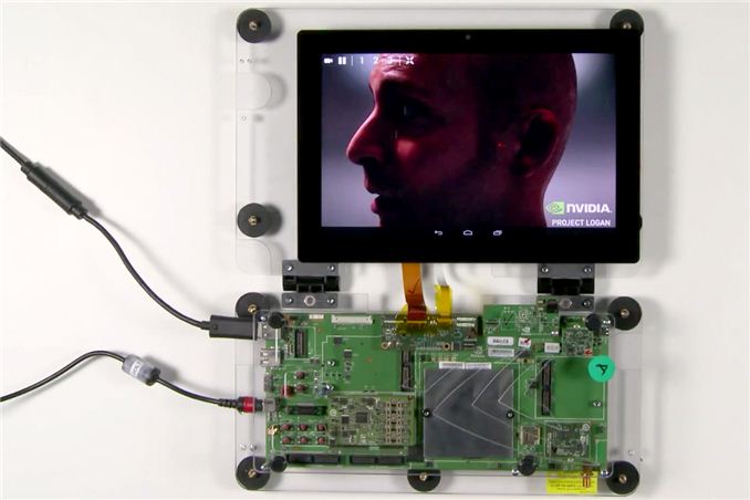
Ever since its arrival in the ultra mobile space, NVIDIA hasn't really flexed its GPU muscle. The Tegra GPUs we've seen thus far have been ok at best, and in serious need of improvement at worst. NVIDIA often blamed an immature OEM ecosystem unwilling to pay for the sort of large die SoCs necessary in order to bring a high-performance GPU to market. Thankfully, that's all changing. Earlier this year NVIDIA laid out its mobile SoC roadmap through 2015, including the 2014 release of Project Logan - the first NVIDIA ultra mobile SoC to feature a Kepler GPU. Yesterday in a private event at Siggraph, NVIDIA demonstrated functional Logan silicon for the very first time.
NVIDIA got Logan silicon back from the fabs around 3 weeks ago, making it almost certain that we're dealing with some form of 28nm silicon here and not early 20nm samples.
NVIDIA isn't talking about CPU cores, but it's safe to assume that Logan will be another 4+1 arrangement of cores - likely still based on ARM's Cortex A15 IP (but perhaps a newer revision of the core). On the GPU front, NVIDIA confirmed our earlier speculation that Logan includes a single Kepler SMX:
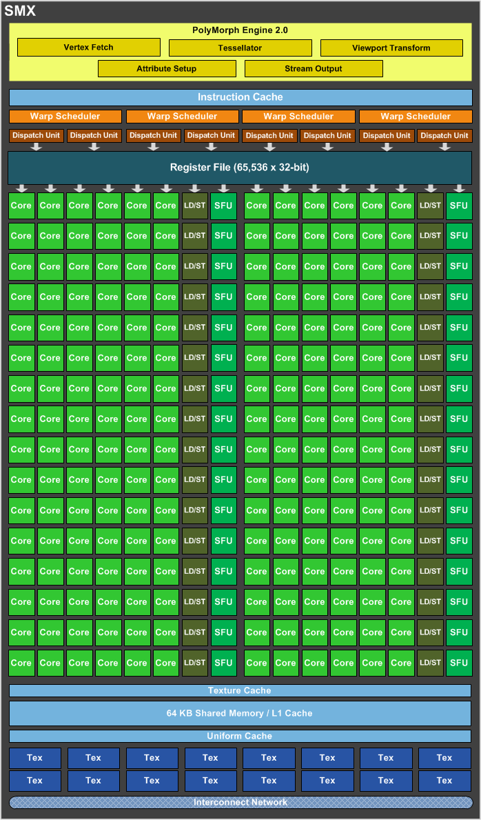
One Kepler SMX features 192 CUDA cores. NVIDIA isn't talking about shipping GPU frequencies either, but it did provide this chart to put Logan's GPU capabilities into perspective:
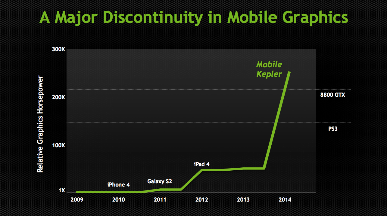
Don't get too excited as we're looking at a comparison of GFLOPS and not game performance, but the peak theoretical ALU bound performance of mobile Kepler should exceed that of a Playstation 3 or GeForce 8800 GTX (memory bandwidth is another story however). If we look closely at NVIDIA's chart and compare mobile Kepler to the iPad 4, we get a better idea of what sort of clock speeds NVIDIA would need to attain this level of performance. Doing some quick Photoshop estimation it looks like NVIDIA is claiming mobile Kepler has somewhere around 5.2x the FP power of the PowerVR SGX 554MP4 in the iPad 4 (76.8 GFLOPS). That works out to be right around 400 GFLOPS. With a 192 core implementation of Kepler, you get 2 FLOPS per core or 384 FLOPS per cycle. To hit 400 GFLOPS you'd need to clock the mobile Kepler GPU at roughly 1GHz. That's certainly doable from an architectural standpoint (although we've never seen it done on any low power 28nm process), but it's probably a bit too high for something like a smartphone.
NVIDIA didn't want to talk frequencies but they did tell me that we might see something this fast in some sort of a tablet. I suspect that most implementations will be clocked significantly lower. Even at half the frequency though, we're still talking about roughly Playstation 3 levels of FP power out of a mobile SoC. We know nothing of Logan's memory subsystem, which obviously plays a major role in real world gaming performance but there's no getting around the fact that Logan's Kepler implementation means serious business. For years we've lamented NVIDIA's mobile GPUs, Logan looks like it's finally going to change that.
API Support and Live Demos
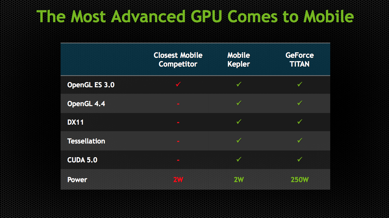
Unlike previous Tegra GPUs, Kepler is a fully unified architecture and OpenGL ES 3.0, OpenGL 4.4 and DirectX 11 compliant. The API compliance alone is a huge step forward for NVIDIA. It's also a big one for game developers looking to move more seriously into mobile. Epic's Tim Sweeney even did a blog post for NVIDIA talking about Logan's implementation of Kepler and how it brings feature parity between PCs, next-gen consoles and mobile platforms. NVIDIA responded in kind by running some Unreal Engine 4 demos on Android on a Logan test platform. That's really the big story behind all of this. With Logan, NVIDIA will bring its mobile GPUs up to feature parity with what it's shipping in the PC market. Game developers looking to port games between console, PC, tablet and smartphone should have an easier job of doing that if all platforms supported the same APIs. Logan will take NVIDIA from being very behind in API support (with no OpenGL ES 3.0 support) to the head of the class.
NVIDIA took its Ira demo, originally run on a Titan at GTC 2013, and got it up and running on a Logan development board. Ira did need some work to make the transition to mobile. The skin shaders were simplified, smaller textures are used and the rendering resolution is dropped to 1080p. NVIDIA claims this demo was done in a 2 - 3W power envelope.
The next demo is called Island and was originally shown on a Fermi desktop part. Running on Logan/mobile Kepler, this demo shows OpenGL 4.3 and hardware tessellation working.
The development board does feature a large heatspreader, but that's not too unusual for early silicon just out of bring up. Logan's package size should be comparable to Tegra 4, although the die size will clearly be larger. The dev board is running Android and is connected to a 10.1-inch 1920 x 1200 touchscreen.


141 Comments
View All Comments
michael2k - Thursday, July 25, 2013 - link
You missed the part where PowerVR 6 is competitive with Logan, but was available for licensing last January. Apple might very well investigate this GPU for their 2014 SoC, but then said SoC would be half as powerful as a PowerVR 6.happycamperjack - Friday, July 26, 2013 - link
I watched some of their demos, seems like PowerVR 6 is designed for mostly for Open GL ES 3.0. I hightly doubt that it can compete with Logan for advance OpenGL 4.x features like tessellation. In fact I'm willing to bet that Logan will have tessellation performance that's more than 3 times faster than PowerVR 6.michael2k - Friday, July 26, 2013 - link
Until HW is available we can't know, but the problem isn't that it can't compete, it's that Logan will come out a year later. So even if Logan is 3 times faster, it will be a year later, and a revised PowerVR 6+ will be out, instead.lmcd - Wednesday, July 24, 2013 - link
We still haven't heard if this has an integrated-enough baseband for all of the lovely USA carriers. I assume it does based on T4i but I don't trust Nvidia on that point.Krysto - Thursday, July 25, 2013 - link
Nvidia uses a (quite revolutionary) soft-modem. All bands can be implemented in the software of the modem.The problem is they've been slow to bring it to market so far (same for Samsung and all the others besides Qualcomm, really). But I doubt this will still be an issue next year.
andyroo77 - Thursday, July 25, 2013 - link
How does this compare to the newest high end PowerVR graphics?As Nvidia will be licensing this design, have they just dealt a death blow to Imagination technologies’ PowerVR/ARM’s Mali/Qualcom’s Adreno lines? It looks pretty good to me but does it blow the latest and greatest from these other companies out the water or is it all marketing hype? Can anyone with the knowledge fill me in?
Krysto - Thursday, July 25, 2013 - link
Kepler might be unmatched, but there's still one way for Nvidia to fail - and that's going with 28nm. They'd be very very stupid to do that, yet they probably will anyway. It's like they haven't learned their lesson with Tegra 3 vs S4 last year.But Tegra 6 with Nvidia's own Denver CPU core and Maxwell GPU - that will also arrive at 16nm FinFET just a year after Logan, should really be KILLER. But there's quite a bit of time until then.
Refuge - Thursday, July 25, 2013 - link
It is waaaaay too late in the story for them to change from 28nm.If they do that then they might as well skip this Tegra and go to the next.
michael2k - Thursday, July 25, 2013 - link
Power VR 6 is the same performance and power envelope as this, but was available to partners last January and should be shipping soon.djgandy - Thursday, July 25, 2013 - link
Same old crap from Nvidia. Nice comparison matrix too. Everyone will support ES 3.0 by the time this comes out. It is Nvidia who left it out of their most recent chip saying it was pointless.As usual they are saying a chip that is not due, for a good year at least, is better than a chip that is based on a 4 year old graphics architecture.