Intel Core i7 4960X (Ivy Bridge E) Review
by Anand Lal Shimpi on September 3, 2013 4:10 AM EST- Posted in
- CPUs
- Intel
- Ivy Bridge
- Ivy Bridge-E
_Die_Wafer_Shot-7845-1_678x452.jpg)
Twenty two months ago Intel launched its LGA-2011 platform and Sandy Bridge E aimed at the high-end desktop enthusiast. The platform brought more cores, more PCIe lanes and more memory bandwidth to those users who needed more than what had become of Intel's performance desktop offerings. It was an acknowledgement of a high end market that seems to have lost importance over the past few years. On the surface, Sandy Bridge E was a very good gesture on Intel's part. Unfortunately, the fact that it's been nearly two years since we first met LGA-2011 without a single architecture update, despite seeing the arrival of both Ivy Bridge and Haswell, doesn't send a great message to the users willing to part with hard earned money to buy into the platform.
Today we see that long awaited update. LGA-2011 remains unchanged, but the processor you plug into the socket moves to 22nm. This is Ivy Bridge Extreme.
Ivy Bridge E: 1.86B Transistors, Up to 6 Cores & 15MB L3
There’s a welcoming amount of simplicity in the Extreme Edition lineup. There are only three parts to worry about:
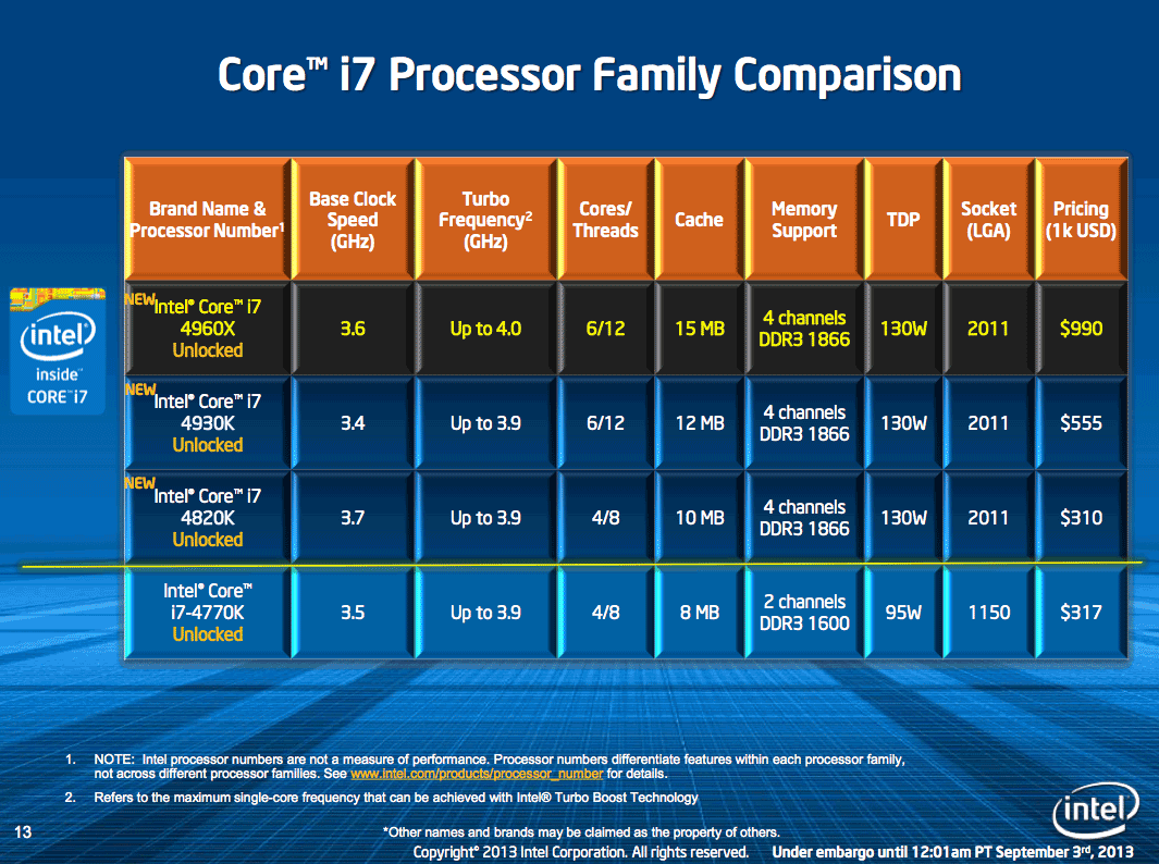
With the exception of the quad-core 4820K, IVB-E launch pricing is identical to what we saw with Sandy Bridge E almost two years ago. The 4820K is slightly cheaper than the highest end Haswell part, but it’s still $25 more expensive than its SNB-E counterpart was at launch. The difference? The 4820 is a K-SKU, meaning it’s fully unlocked, and thus comes with a small price premium.
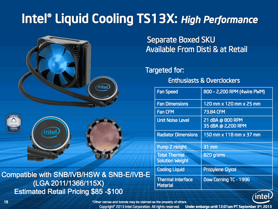
All of the IVB-E parts ship fully unlocked, and are generally capable of reaching the same turbo frequencies as their predecessors. The Core i7-4960X and the i7-3970X before it, are the only Intel CPUs officially rated for frequencies of up to 4GHz (although we’ve long been able to surpass that via overclocking). Just as before, none of these parts ship with any sort of cooling (because profit), you'll need to buy a heatsink/fan or closed loop water cooler separately. Intel does offer a new cooler for IVB-E, the TS13X:
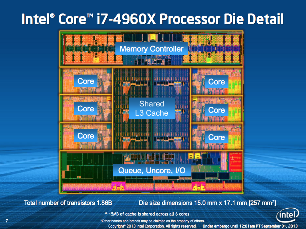
While Sandy Bridge E was an 8-core die with two cores disabled, Ivy Bridge E shows up in a native 6-core version. There’s no die harvesting going on here, all of the transistors on the chip are fully functional. The result is a significant reduction in die area, from the insanity that was SNB-E’s 435mm2 down to an almost desktop-like 257mm2.
| CPU Specification Comparison | |||||||||
| CPU | Manufacturing Process | Cores | GPU | Transistor Count (Schematic) | Die Size | ||||
| Haswell GT3 4C | 22nm | 4 | GT3 | ? | 264mm2 (est) | ||||
| Haswell GT2 4C | 22nm | 4 | GT2 | 1.4B | 177mm2 | ||||
| Haswell ULT GT3 2C | 22nm | 2 | GT3 | 1.3B | 181mm2 | ||||
| Intel Ivy Bridge E 6C | 22nm | 6 | N/A | 1.86B | 257mm2 | ||||
| Intel Ivy Bridge 4C | 22nm | 4 | GT2 | 1.2B | 160mm2 | ||||
| Intel Sandy Bridge E 6C | 32nm | 6 | N/A | 2.27B | 435mm2 | ||||
| Intel Sandy Bridge 4C | 32nm | 4 | GT2 | 995M | 216mm2 | ||||
| Intel Lynnfield 4C | 45nm | 4 | N/A | 774M | 296mm2 | ||||
| AMD Trinity 4C | 32nm | 4 | 7660D | 1.303B | 246mm2 | ||||
| AMD Vishera 8C | 32nm | 8 | N/A | 1.2B | 315mm2 | ||||
Cache sizes remain unchanged. The highest end SKU features a full 15MB L3 cache, while the mid-range SKU comes with 12MB and the entry-level quad-core part only has 10MB. Intel adds official support for DDR3-1866 (1 DIMM per channel) with IVB-E, up from DDR3-1600 in SNB-E and Haswell.
TDPs all top out at 130W, bringing back memories of the high-end desktop SKUs of yesterday. Obviously these days much of what we consider to be high-end exists below 100W.
Of course processor graphics is a no-show on IVB-E. As IVB-E retains the same socket as SNB-E, there are physically no pins set aside for things like video output. Surprisingly enough, early rumors indicate Haswell E will also ship without an integrated GPU.
The Extreme Cadence & Validated PCIe 3.0
Understanding why we’re talking about Ivy Bridge E now instead of Haswell E is pretty simple. The Extreme desktop parts come from the Xeon family. Sandy Bridge E was nothing more than a 6-core Sandy Bridge EP variant (Xeon E5), and Ivy Bridge E is the same. In the Xeon space, the big server customers require that Intel keep each socket around for at least two generations to increase the longevity of their platform investment. As a result we got two generations of Xeon CPUs (SNB-E/EP, and IVB-E/EP) that leverage LGA-2011. Because of when SNB-E was introduced, the LGA-2011 family ends up out of phase with the desktop/notebook architectures by around a year. So we get IVB-E in 2013 while desktop/notebook customers get Haswell. Next year when the PC clients move to 14nm Broadwell, the server (and extreme desktop) customers will get 22nm Haswell-E.
The only immediate solution to this problem would be for the server parts to skip a generation - either skip IVB-E and go to Haswell-E (not feasible as that would violate the 2 generations rule above), or skip Haswell-E and go directly to Broadwell-E next year. Intel tends to want to get the most use out of each one of its architectures, so I don’t see a burning desire to skip an architecture.
Server customers are more obsessed with core counts than modest increases in IPC, so I don’t see a lot of complaining there. On the desktop however, Ivy Bridge E poses a more interesting set of tradeoffs.
The big advantages that IVB-E brings to the table are a ridiculous number of PCIe lanes, a quad-channel memory interface and 2 more cores in its highest end configuration.
While the standard desktop Sandy Bridge, Ivy Bridge and Haswell parts all feature 16 PCIe lanes from the CPU’s native PCIe controller, the Extreme parts (SNB-E/IVB-E) have more than twice that.
There are 40 total PCIe 3.0 lanes that branch off of Ivy Bridge E. Since IVB-E and SNB-E are socket compatible, that’s the same number of lanes we got last time. The difference this time around is IVB-E’s PCIe controller has been fully validated with PCIe 3.0 devices. While Sandy Bridge E technically supported PCIe 3.0 the controller was finalized prior to PCIe 3.0 devices being on the market and thus wasn’t validated with any of them. The most famous case being NVIDIA’s Kepler cards which by default run in PCIe 2.0 mode on SNB-E systems. Forcing PCIe 3.0 mode on SNB-E worked in many cases, while in others you’d see instability.
NVIDIA tells us that it plans to enable PCIe 3.0 on all IVB-E systems. Current drivers (including the 326.80 beta driver) treat IVB-E like SNB-E and force all Kepler cards to PCIe 2.0 mode, but NVIDIA has a new driver going through QA right now that will default to PCIe 3.0 when it detects IVB-E. SNB-E systems will continue to run in PCIe 2.0 mode.


Intel’s X79: Here for One More Round
Unlike its mainstream counterpart, Ivy Bridge E does not come with a new chipset. That’s right, not only is IVB-E socket compatible with SNB-E, it ships with the very same chipset: X79.
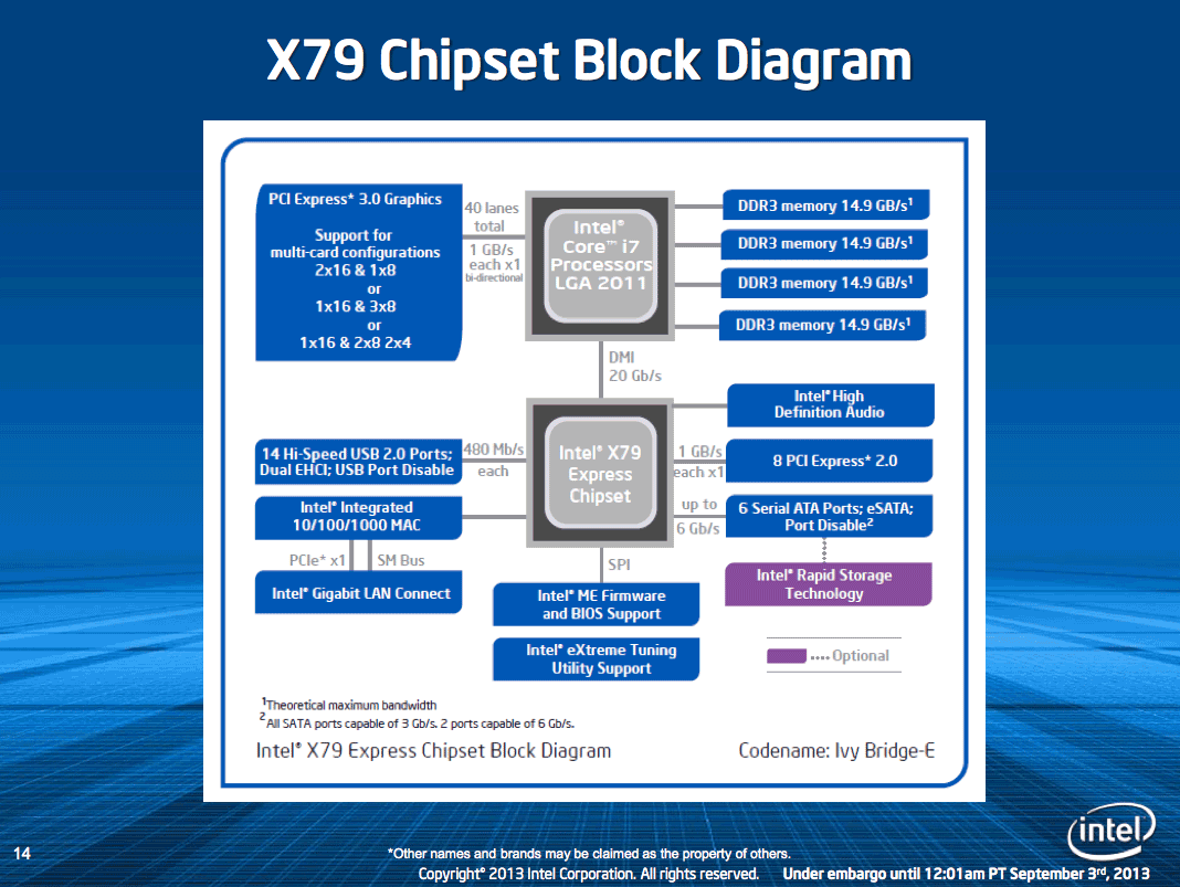
As a refresher Intel’s X79 chipset has no native USB 3.0 support and only features two native 6Gbps SATA ports. Motherboard makers have worked around X79’s limitations for years now by adding a plethora of 3rd party controllers. I personally prefer Intel’s native solutions to those we find from 3rd parties, but with X79 you’ve got no choice.
The good news is that almost all existing X79 motherboards will see BIOS/EFI updates enabling Ivy Bridge E support. The keyword there is almost.
When it exited the desktop motherboard market, Intel only promised to release new Haswell motherboards and to support them through the end of their warranty period. Intel never promised to release updated X79 motherboards for Ivy Bridge E, nor did it promise to update its existing X79 boards to support the new chips. In a very disappointing move, Intel confirmed to me that none of its own X79 boards will support Ivy Bridge E. I confirmed this myself by trying to boot a Core i7-4960X on my Intel DX79SI - the system wouldn’t POST. While most existing X79 motherboards will receive BIOS updates enabling IVB-E support, anyone who bought an Intel branded X79 motherboard is out of luck. Given that LGA-2011 owners are by definition some of the most profitable/influential/dedicated customers Intel has, I don’t think I need to point out how damaging this is to customer relations. If it’s any consolation, IVB-E doesn’t actually offer much of a performance boost over SNB-E - so if you’re stuck with an Intel X79 motherboard without IVB-E support, you’re not missing out on too much.
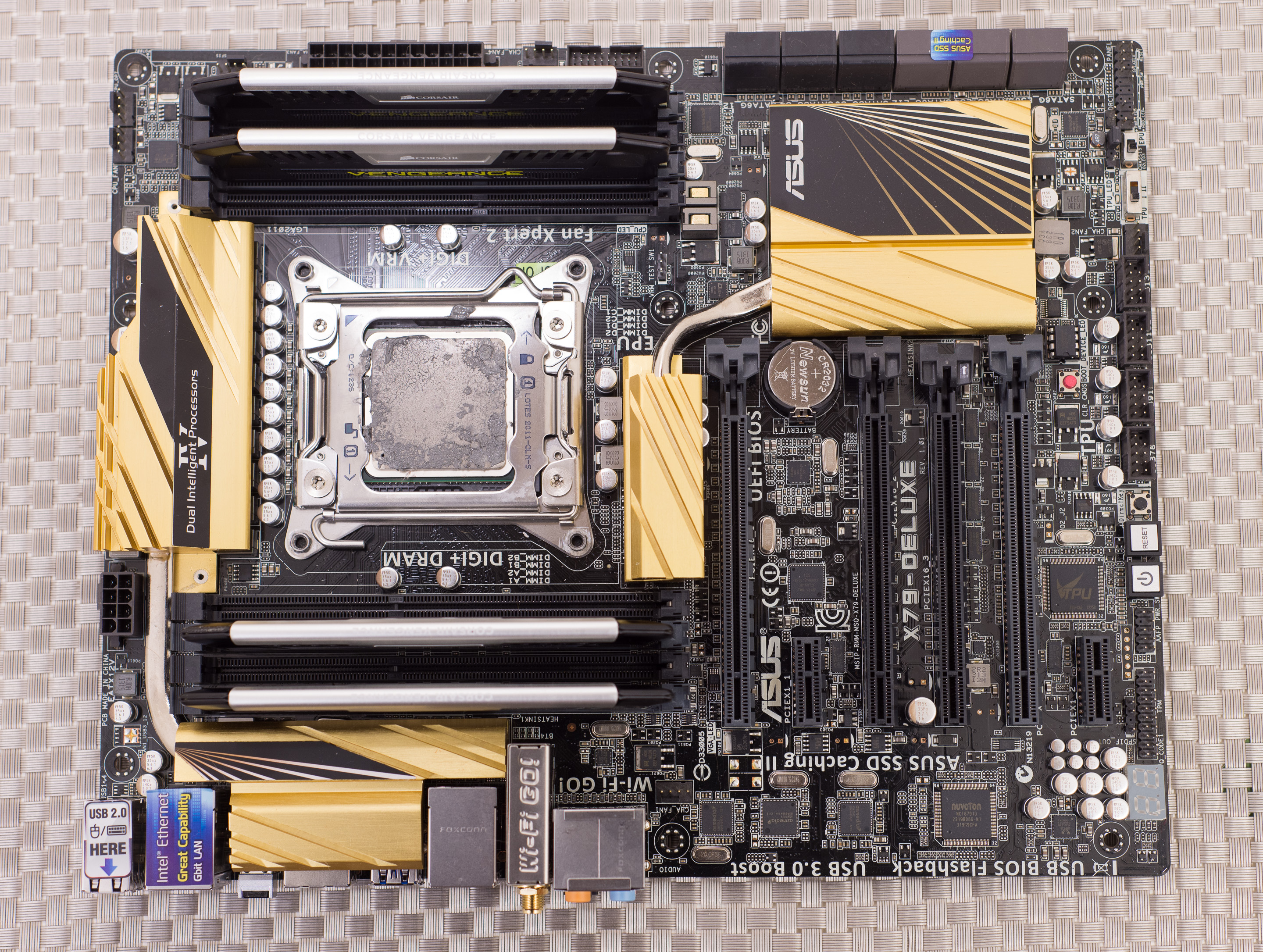
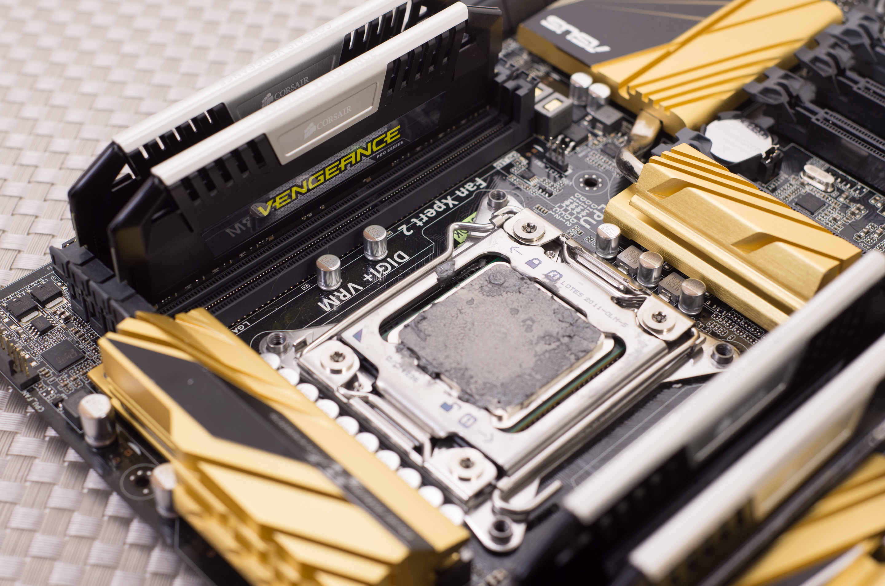
The Testbed: ASUS’ New X79 Deluxe
As all of my previous X79 boards were made by Intel, I actually had no LGA-2011 motherboards that would work with IVB-E on hand. ASUS sent over the latest revision of its X79 Deluxe board with official IVB-E support:
The board worked relatively well but it seems like there’s still some work that needs to be done on the BIOS side. When loaded with 32GB of RAM I saw infrequent instability at stock voltages. It’s my understanding that Intel didn’t provide final BIOS code to the motherboard makers until a couple of weeks ago, so don’t be too surprised if there are some early teething pains. For what it’s worth, that this makes Ivy Bridge E the second high-end desktop launch in a row that hasn’t gone according to Intel’s previously high standards.
Corsair supplied the AX1200i PSU and 4 x 8GB DDR3-1866 Vengeance Pro memory for the testbed.
For more comparisons be sure to check out our performance database: Bench.
| Testbed Configurations | ||||
| Motherboard(s) |
ASUS X79 Deluxe
ASUS P8Z77-V Deluxe ASUS Crosshair V Formula Intel DX58SO2 |
|||
| Memory |
Corsair Vengeance DDR3-1866 9-10-9-27
|
|||
| SSD |
Corsair Neutron GTX 240GB
OCZ Agility 3 240GB OCZ Vertex 3 240GB |
|||
| Video Card |
NVIDIA GeForce GTX Titan x 2 (only 1 used for power tests)
|
|||
| PSU |
Corsair AX1200i
|
|||
| OS |
Windows 8 64-bit
Windows 7 64-bit Windows Vista 32-bit (for older benchmarks) |
|||


120 Comments
View All Comments
1Angelreloaded - Tuesday, September 3, 2013 - link
Can you have a comparison chart please for the 4770k, E5-8core Xenon, 4960X, with benchmarks included. This kind of makes little sense to me X-79 was behind on feature sets like full SATA3 when in reality a lot of these boards will be used as workstation/normal/gaming computers, performance on those boards tends to suffer because lack there of native support. Instead 3rd party chips are used to add extra features which have significant drawbacks. I understand using the socket for 2 gen in order to extend life of boards however 1336 and the next leap to haswell should have been taken, making a board last 2 years with the prime features that defined that generation. This just seams like intel is ignoring its higher end market due to lack of competition out there.sabarjp - Tuesday, September 3, 2013 - link
Kind of depressing that 3 years of technology only took the compile of Firefox from 23 minutes to 20 minutes. The high-end isn't looking so high these days.dgingeri - Tuesday, September 3, 2013 - link
So where's the 4820k review? I don't care much about more than 4 cores, but I need more I/O than Haswell offers. (crappy motherboards that offer either 8/4/4 or 8/8/2 are just unacceptable.) I'd like to know how the 4820k overclocks and handles I/O from dual and triple SLi/Crossfire.Eidigean - Tuesday, September 3, 2013 - link
Visual Studio unfortunately does not compile in parallel the way you might think. In a solution you may have multiple projects. If one project depends on four other projects, those four will be compiled in parallel; one project per thread. Once the four dependencies are built, it can build the fifth; however, that last project will be built single-threaded.Xcode and native Android projects (with gcc) can actually build multiple files from one project in parallel. On an i7 with hyperthreading, all eight logical processors can build up to eight files simultaneously. This scales with more cores very nicely.
In summary, VS builds multiple projects from one solution in parallel, while gcc builds multiple files from one project in parallel; the latter of which is much faster.
I'm curious now to see the build times of Firefox for Mac on a rMBP with an i7. Eagerly waiting for a 12 core Mac Pro with 24 logical processors.
BrightCandle - Tuesday, September 3, 2013 - link
Visual Studio is a very poor parallel compilation test. GCC with make -p can really utilise a lot more cores but its not very Windows like to use GCC (although I suspect many developers do that).I haven't found many Java builds doing well on multiple cores, and neither Scala. Its the unit tests where I get the cores going, I can saturate hundreds of cores with unit tests if I had them, and since I run them in the background on every change I certainly do get a lot of usage out of the extra cores. But a clean compile is not one of those cases where I see any benefit from the 6 cores. Of course I would hope these days we don't do that very often.
althaz - Tuesday, September 3, 2013 - link
It is a poor parallel test, but it is a fantastic real-world test for a lot of devs.madmilk - Tuesday, September 3, 2013 - link
About 25 minutes here on an 2.6GHz/16GB rMBP. Pretty much as expected for quad Ivy Bridge.bminor13 - Tuesday, September 3, 2013 - link
Parallel file-level compilation is possible in VS2010 and up with the /MP project switch. This is not enabled by default I believe for compatibility reasons.BSMonitor - Tuesday, September 3, 2013 - link
A Haswell-E will most likely bring a different pin-count, correct?? So this X79 is a dead end platform any way you look at it. Buying the Quad IVB-E makes almost no sense whatsoever.Casper42 - Tuesday, September 3, 2013 - link
Most Intel chips use a Tick Tock release cycle. Tick Tock Tick Tock Tick Tock etcTick is an Incremental upgrade. Same socket and largely same design, but reduced lithography (32nm down to 22nm for example). Sometimes new Instructions but often not.
Tock is an Overhaul upgrade. Uses same Lithography as the previous gen, but is a new internal architecture, often a new Socket, and where most new Instruction sets show up.
Then you get another Tick.
Core 2/Conroe was a Tock and was 65nm
Core 2/Penryn was a Tick and was 45nm
Core iX/Nehalem was a Tock and was 45nm
Core iX/Westmere was a Tick and was 32nm
Core iX/Sandy Br was a Tock and was 32nm
Core iX/Ivy Bridge is a Tick and is 22nm
Core iX/Haswell is a Tock and is 22nm
So to say that X79 is a dead platform should not really be a shock to anyone. They got Sandy and Ivy out of it. Thats 1 Tock and 1 Tick and now its time to move on. They do this exact same thing in the 2P Server market where people spend $10K or more per server. The fact of the matter is the server market has already pretty much learned. Don't bother upgrading that server/machine, just ride it for 3-4 years and then replace it completely. SATA, Memory and CPUs have all changed enough by then you want to reset everything anyway.