Chipworks Confirms Xbox One SoC Has 14 CUs with 2 Disabled
by Anand Lal Shimpi on November 26, 2013 8:57 PM EST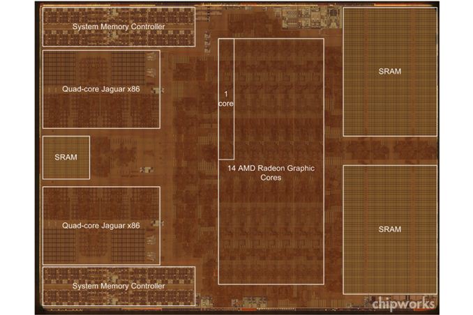
In our mini-review of the Xbox One I speculated that the shipping version of Microsoft's console featured 14 AMD GCN CUs (Graphics Core Next Compute Units), with two disabled to improve yields. Microsoft publicly stated that Xbox One development kits featured 14 CUs and Sony similarly had 20 CUs with only 18 enabled with the PS4. With Xbox One hardware in the wild, Chipworks went to task delayering the SoC/APU and confirmed the speculation - the Xbox One does indeed feature 14 CUs (pictured above).
Microsoft claims it weighed the benefits of running 12 CUs (768 cores) at 853MHz vs. 14 CUs (896 cores) at 800MHz and decided on the former. Given that the Xbox One APU only features 16 ROPs and ROP performance scales with clock speed, Microsoft likely made the right decision. Thermal and yield limits likely kept Microsoft from doing both - enabling all CUs and running them at a higher frequency. Chances are that over time Microsoft will phase out the extra CUs, although it may take a while to get there. I'm not sure if we'll see either company move to 20nm, they may wait until 14/16nm in order to realize real area/cost savings which would mean at least another year of shipping 14/20 CU parts at 28nm.
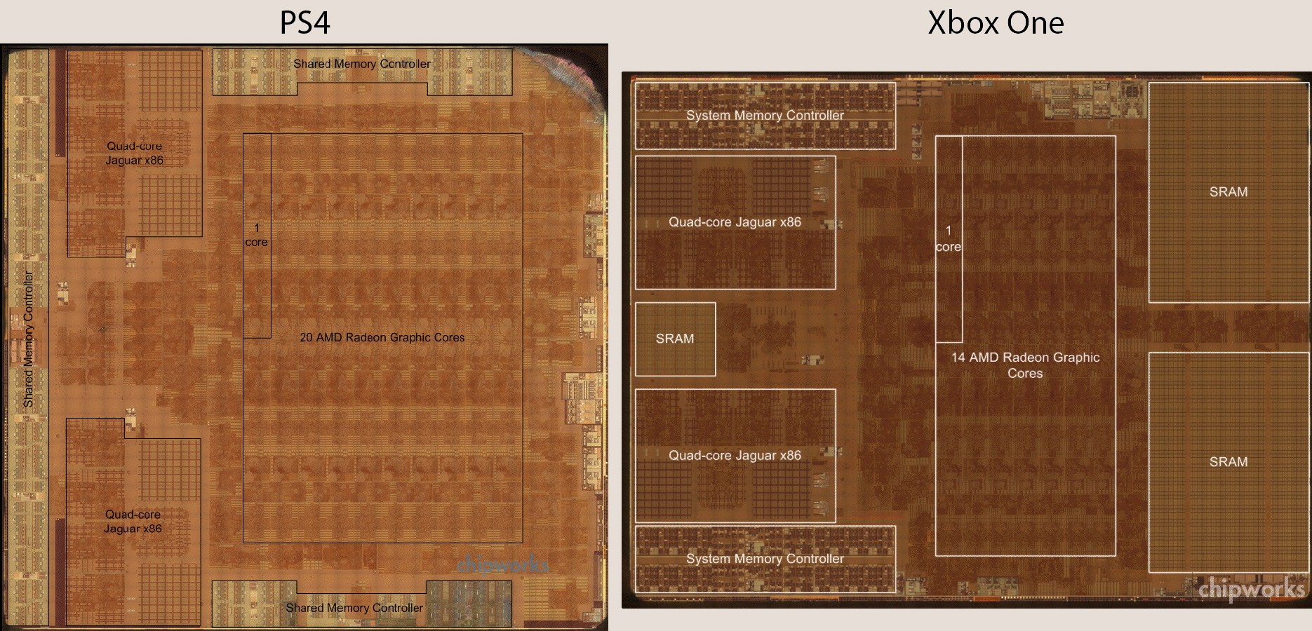
Compared to the PS4's APU, we see a very similar layout. The on-die SRAM sits next to the GPU array, and far away from the CPU, which makes sense given that the latter isn't allowed direct access to the eSRAM. You can very clearly see the tradeoff Microsoft had to make in order to accommodate its eSRAM. The GPU area shrinks considerably.


47 Comments
View All Comments
TheinsanegamerN - Monday, December 2, 2013 - link
i should also point out, that if the one had 40 compute units, it would have double the gpu hardware of the ps4.mikk - Wednesday, November 27, 2013 - link
"I'm not sure if we'll see either company move to 20nm, they may wait until 14/16nm in order to realize real area/cost savings"This part doesn't make sense, there is no area scaling and cost saving with 16nm from TSMC, it's a 20nm Finfet process without area scaling.
Gabrielsp85 - Wednesday, November 27, 2013 - link
There any way to point where the 50MCU the architects said the X1 had are??? also when you scale X1 and PS4 SoC, the X1 GPU cores are bigger, does that mean anything??tipoo - Thursday, November 28, 2013 - link
Different layout optimizations probably. But I think the One CUs were actually shorter when scaled.Gabrielsp85 - Friday, November 29, 2013 - link
They are actually longer, I'll share a picture when I find it, could also mean X1 use a newer version of GCN?pliiny - Thursday, December 5, 2013 - link
Anyone think the SRAM on the Xbox one soc is related to the Mantle API?pliiny - Thursday, December 5, 2013 - link
Does anyone think the eSRAM on the xbox one soc is related to the Mantle API?