Imagination's PowerVR Rogue Architecture Explored
by Ryan Smith on February 24, 2014 3:00 AM EST- Posted in
- GPUs
- Imagination Technologies
- PowerVR
- PowerVR Series6
- SoCs
When it comes to our coverage of SoCs, one aspect we’ve been trying to improve on for some time now is our coverage and understanding of the GPU portion of those SoCs. In the PC space we’re fortunate that there are just three major players – Intel, NVIDIA, and AMD – and that all three of them have over the years learned how to become very open and forthcoming about their GPU architectures. As a result we’ve had a level of access that has allowed us to better understand PC GPUs in a way that in earlier times simply wasn’t possible.
In the SoC space however we haven’t been so fortunate. Our understanding of most SoC GPU architectures has not been nearly as deep due to the fact that SoC GPU designers have been less willing to come forward with public details about their architectures and how those architectures have evolved over the years. And this has been for what’s arguably a good reason – unlike the PC GPU space, where only 2 of the 3 players compete in either the iGPU or dGPU markets, in the SoC GPU space there are no fewer than 7 players, all of whom are competing in one manner or another: NVIDIA, Imagination Technologies, Intel, ARM, Qualcomm, Broadcom, and Vivante.
Some of these players use their designs internally while others license out their designs as IP for inclusion in 3rd party SoCs, but all these players are in a much more competitive market that is in a younger place in its life. All the while SoC GPU development still happens at a relatively quick pace (by GPU standards), leading to similarly quick turnarounds between GPU generations as GPU complexity has not yet stretched out development to a 3-4 year process. As a result of SoC GPUs still being a young and highly competitive market, it’s a foregone conclusion that there is still a period of consolidation ahead of us – not unlike what has happened to SoC integrators such as TI – which provides all the more reason for SoC GPU players to be conservative about providing public details about their architectures.
With that said, over the years we have made some progress in getting access to the technical details, due in large part to the existing openness policies of NVIDIA and Intel. Nevertheless, as two of the smaller players in the mobile GPU space this still leaves us with few details on the architectures behind the majority of SoC GPUs. We still want more.
This brings us to today. In what should prove to be an extremely eventful and important day for our coverage and understanding of SoC GPUs, we’d like to welcome Imagination Technologies to the “open architecture” table. Imagination chosen to share more details about the inner workings of their Rogue Series 6 and Series 6XT architectures, thereby giving us our first in-depth look at the architecture that’s powering a number of high-end products (not the least of which is all of Apple’s current-gen products) and descended from some of the most widely used SoC GPU designs of all time.

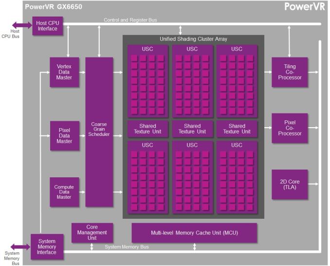
Now Imagination is not going to be sharing everything with us today. The bulk of the details Imagination is making available relate to their Unified Shading Cluster (USC) shading block, the heart of the Series 6/6XT GPUs. They aren’t discussing other aspects of their designs such as their geometry processors, cache structure, or Tile Based Deferred Rendering system – the company’s secret sauce and most potent weapon for SoC efficiency – but hopefully one day we’ll get there. In the meantime we will have our hands full just taking our first look at the Series 6/6XT USCs.
Finally, before we begin we’d like to thank Imagination for giving us this opportunity to evaluate their architecture in such great detail. We’ve been pushing for this for quite some time, so we’re pleased that this is coming to pass.
Imagination is publishing a pair of blogs and pseudo whitepapers on their website today: Graphics cores: trying to compare apples to apples, and PowerVR GX6650: redefining performance in mobile with 192 cores. Along with this they have also been answering many of our deepest technical questions, so we should have a good handle on the Rogue USC. So with that in mind, let’s dive in.


95 Comments
View All Comments
dragonsqrrl - Tuesday, February 25, 2014 - link
... and the 64-bit architecture in the A7 is a completely different story. Apple wasn't first to market with 64-bit because they had an accelerated development schedule compared to other chipmakers. Apple was first to market because they started development first, ahead of everyone else.Apple doesn't develop Series 6, they license it, and we know when it becomes available for integration and when devices based on it come to market. We also know how long it usually takes between tapeout of an SOC, production, and final availability in devices, and based on this it would be very difficult if not impossible for Apple to put a 6XT in the A8 if they keep to their regular release schedule. I think going from an ~18 to ~8 month schedule is a bit much even for Apple, especially considering the new process shrink.
michael2k - Wednesday, February 26, 2014 - link
It's available for license now. Doesn't that normally mean that, as soon as the computer finishes synthesizing the design, it can be taped out now as well? The issue then is how much work needs to be done to get the design to work at the desired power envelope and clock, and if said work is worth it.Samus - Monday, February 24, 2014 - link
Considering the highly parallel nature of graphics processing, PowerVR's low core count and non-linear arrangement will make then weak in real-world gaming but strong in synthetic GFLOPS since their cores are stronger.For example, ATI has the weakest GPU cores of everybody but they cram over 2000 onto a GPU, seems to be doing pretty good for their performance.
michael2k - Tuesday, February 25, 2014 - link
Your example is irrelevant since ATI has no mobile solution and PowerVR has been the strongest in real world gaming since, well, until the K1 ships, PowerVR has had no real competition.Adreno is technically competent, but Qualcomm isn't seeking to push their transistor budget too high.
extide - Friday, February 28, 2014 - link
Wow, so you basically didn't read the article at all did you? This nonsense is exactly what this article is trying to prevent. Lol.Anders CT - Tuesday, February 25, 2014 - link
And what chip is using a GX6650 GPU? None existing that I know of.The Tegra K1 is a chip. Kepler and PowerVR 6XT is GPU architectures. And kepler has been around for several years.
dragonsqrrl - Wednesday, February 26, 2014 - link
Not sure how to respond to this, other than you completely misinterpreted my comment.dragonsqrrl - Wednesday, February 26, 2014 - link
Apologies, you weren't responding to my comment. I was wondering why it made no sense in the context of what I said.The comments section on Anandtech makes it really difficult sometimes to see who's responding to who, especially when it gets really long like this.
Sonicadvance1 - Monday, February 24, 2014 - link
So they have 2x Float32 ALU cores, 4x Float16 ALU cores, and a SFU core.This has no mention of Integer cores.
Am I to assume that integers won't run on the F32/F16 cores but instead of the SFU core so using integers will be 1/6th the speed of floats?
Seems like a large drawback, Mali and Adreno both run integers at the same speed as 32bit floats.
ryszu - Monday, February 24, 2014 - link
Integer happens on the F32 hardware.