Samsung SSD 850 Pro (128GB, 256GB & 1TB) Review: Enter the 3D Era
by Kristian Vättö on July 1, 2014 10:00 AM EST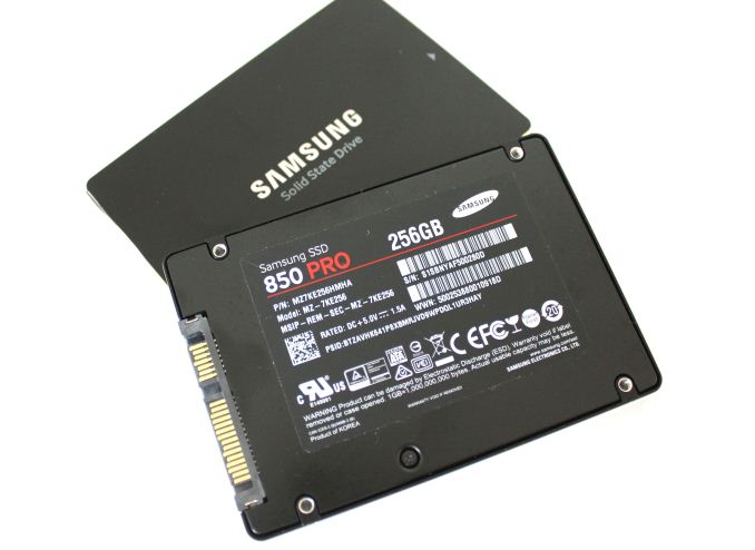
Over the last three years, Samsung has become one of the most dominant players in the SSD industry. Samsung's strategy has been tight vertical integration ever since the beginning, which gives Samsung the ability to be in the forefront of new technologies. That is a massive advantage because ultimately all the parts need to be designed and optimized to work properly together. The first fruit of Samsung's vertical integration was the SSD 840, which was the first mass produced SSD to utilize TLC NAND and gave Samsung a substantial cost advantage. Even today, the SSD 840 and its successor, the 840 EVO, are still the only TLC NAND based SSDs shipping in high volume. Now, two years later, Samsung is doing it again with the introduction of the SSD 850 Pro, the world's first consumer SSD with 3D NAND.
For years it has been known that the scalability of traditional NAND is coming to an end. Every die shrink has been more difficult than the previous as the endurance and performance have decreased with every node, making it less and less efficient to scale the size down. Scaling below 20nm was seemed as a major obstacle but the industry was able to cross that with some clever innovations in the NAND design. However, the magic hat is now running out of tricks and a more signficant change to the NAND design is required to keep scaling the cost.
The present solution to the scalability problem is 3D NAND, or V-NAND as Samsung calls it. Traditionally NAND and other semiconductors are scaled horizontally along the X and Y axes but due to the laws of physics, there is a limit of how small the transistors can be made. To solve the problem, 3D NAND introduces a Z-axis i.e. a vertical dimension. Instead of cramming transistors horizontally closer and closer to each other, 3D NAND stacks layers of transistors on top of each other. I will be going through the structure and characteristics of 3D NAND in detail over the next few pages.
By stacking transistors (i.e. cells when speaking about NAND) vertically, Samsung is able to relax the process node back to a much more convenient 40nm. When there are 32 cells on top of each other, it is obvious that there is no need for a 10nm-class node because the stacking increases the density, allowing production costs to scale lower. As we have seen with the history of NAND die shrinks, a higher process node provides more endurance and higher performance, which is what the 850 Pro and V-NAND is all about.
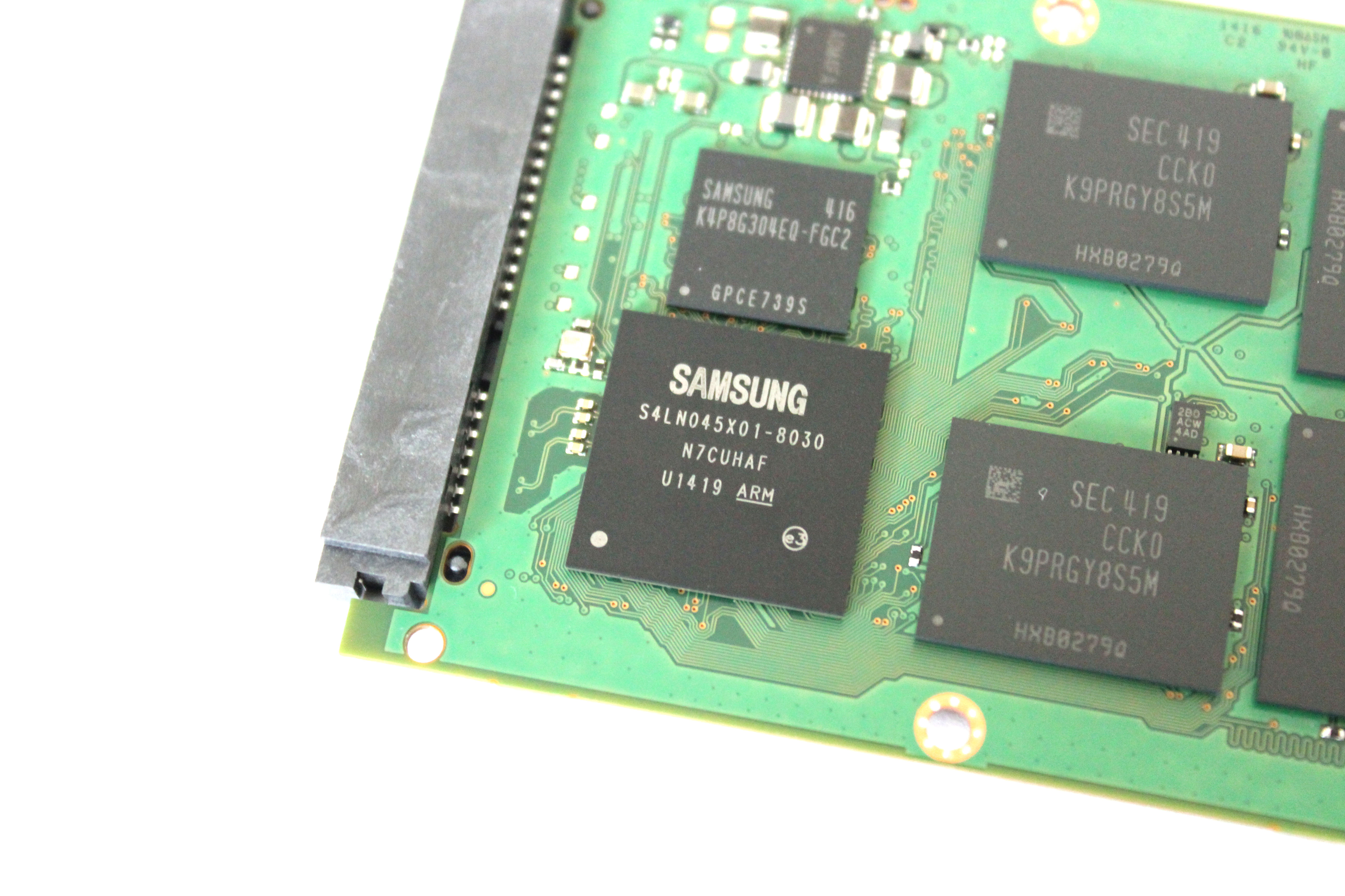
Fundamentally the only change in the 850 Pro is the switch to V-NAND. The interface is still SATA 6Gbps and the controller is the same triple-core MEX from the 840 EVO, although I am still waiting to hear back from Samsung whether the clock speed is the same 400MHz. The firmware, on the other hand, has gone through a massive overhaul to adopt the characteristics of V-NAND. With shorter read, program and erase latencies and higher endurance, the firmware needs to be properly optimized or otherwise the full benefits of V-NAND cannot be utilized.
I bet many of you would have liked to see the 850 Pro move to the PCIe interface but I understand Samsung's decision to hold off with PCIe for a little while longer. The market for aftermarket PCIe SSDs is still relatively small as the PC industry is figuring out how to adopt the new interface, so for the time being Samsung is fine with watching from the side. The XP941 is and will continue to be available to the PC OEMs but for now Samsung will be keeping it that way. From what I have heard, Samsung could bring the XP941 to the retail market rather quickly if needed but Samsung has always been more interested in the high volume mainstream market instead of playing in the niches.
| Samsung SSD 850 Pro Specifications | ||||
| Capacity | 128GB | 256GB | 512GB | 1TB |
| Controller | Samsung MEX | |||
| NAND | Samsung 2nd Gen 86Gbit 40nm MLC V-NAND | |||
| DRAM (LPDDR2) | 256MB | 512MB | 512MB | 1GB |
| Sequential Read | 550MB/s | 550MB/s | 550MB/s | 550MB/s |
| Sequential Write | 470MB/s | 520MB/s | 520MB/s | 520MB/s |
| 4KB Random Read | 100K IOPS | 100K IOPS | 100K IOPS | 100K IOPS |
| 4KB Random Write | 90K IOPS | 90K IOPS | 90K IOPS | 90K IOPS |
| Power | 2mW (DevSLP) / 3.3W (read) / 3.0W (write) | |||
| Encryption | AES-256, TCG Opal 2.0 & IEEE-1667 (eDrive supported) | |||
| Endurance | 150TB | |||
| Warranty | 10 years | |||
| Availability | July 21st | |||
The performance figures in the table above give us the first glimpse of what V-NAND is capable of. Typically modern 128GB SSDs are only good for about 300MB/s but the 850 Pro is very close to saturating the SATA 6Gbps bus even at the smallest capacity. This is due to the much lower program times of V-NAND because write performance has been bound by NAND performance for quite some time now.
| Endurance Comparison of High-End SSDs | |||
| Samsung SSD 850 Pro | Intel SSD 730 | SanDisk Extreme Pro | OCZ Vector 150 |
| 150TB |
91TB (240GB) 128TB (480GB) |
80TB | 91TB |
The other major improvement from V-NAND is the endurance. All capacities, including the smallest 128GB, are rated at 150TB, which is noticeably higher than what any other consumer-grade SSD offers. Moreover, Samsung told me that the endurance figure is mainly meant to separate the 850 Pro from the enterprise drives to guide enterprise clients to the more appropriate (and expensive) drives as the 850 Pro does not have power loss protection or end-to-end data protection for example. However, I was told that the warranty is not automatically denied if 150TB is reached under a client workload. In fact, Samsung said that they have a 128GB 850 Pro in their internal testing with over eight petabytes (that is 8,000TB) of writes and the drive still keeps going, so I tip my hat to the person who is able to wear out an 850 Pro in a client environment during my lifetime.
Another interesting aspect of V-NAND is its odd capacity per die. Traditionally NAND capacies have come in powers of two, such as 64Gbit and 128Gbit, but with V-NAND Samsung is putting an end to that trend. The second generation 32-layer V-NAND comes in at 86Gbit or 10.75GB if you prefer the gigabyte form. I will be covering the reason behind that in more detail when we look at V-NAND more closely in the next few pages but as far as I know there has never been a strict rule as to why the capacities have scaled in powers of two. I believe it is just a relic from the old days that has stayed in the memory industry because deep down binary is based on powers of two but the abnormal die capacity should have no effect on the operation of the NAND or the SSD as long as everything is optimized for it.
| NAND Configurations | ||||
| 128GB | 256GB | 512GB | 1TB | |
| # of NAND Packages | 4 (?) | 4 | 8 (?) | 8 |
| Package Configurations |
2 x 4 x 86Gbit 2 x 2 x 86Gbit |
2 x 8 x 86Gbit 2 x 4 x 86Gbit |
4 x 8 x 86Gbit 4 x 4 x 86Gbit |
4 x 16 x 86Gbit 4 x 8 x 86Gbit |
| Raw NAND Capacity | 129GiB | 258GiB | 516GiB | 1032GiB |
| Over-Provisioning | 7.6% | 7.6% | 7.6% | 7.6% |
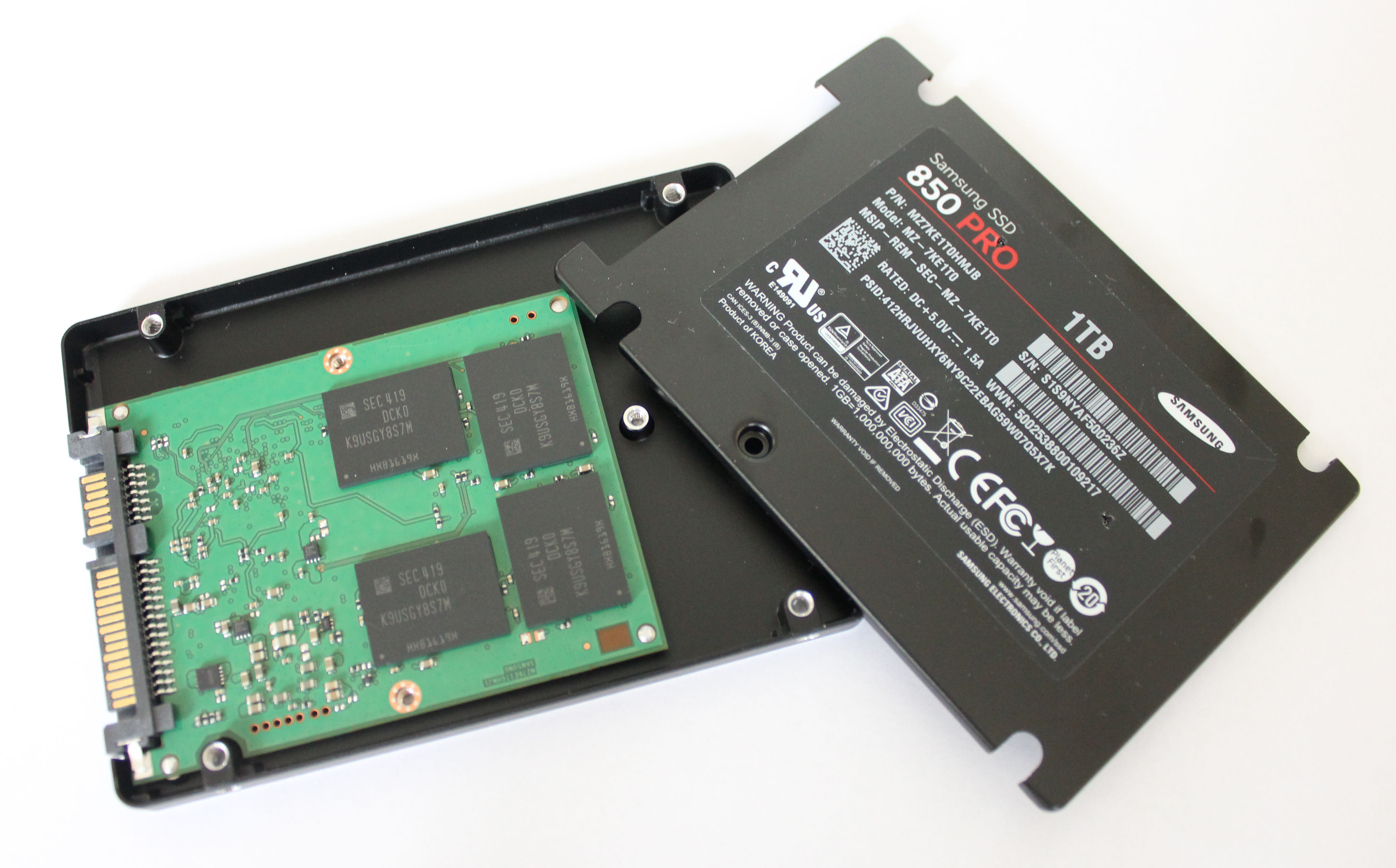
Due to the odd die capacity, the die configurations are also quite unusual. I found two different capacity packages inside my review samples and with Samsung’s NAND part decoder I was able to figure out the die configurations for each capacity. Unfortunately, Samsung did not send us the 512GB model and I could not get the 128GB model open as Samsung uses pentalobe Torx screws and I managed to wear out the screw while trying to open it with an inappropriate screw driver (it worked for the other models, though), so thus there are question marks at those capacities in the table. However, this should not impact the raw NAND capacities as long as all capacities follow the same 7.6% over-provisioning trend but the package configurations may be different. I will provide an update once I receive a confirmation from Samsung regarding the exact configurations for each capacity.
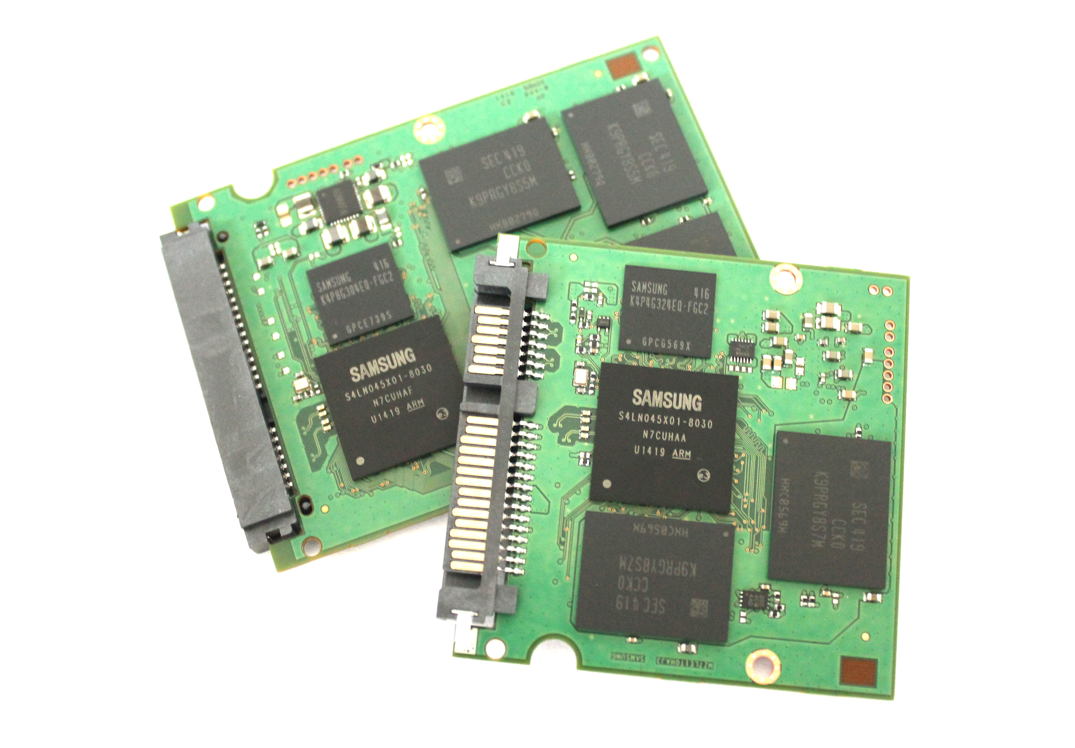
The 850 Pro also switches to smaller PCB designs. The PCB in the 1TB model populates around two thirds of the area of the chassis, while the 256GB PCB comes in at even smaller size. The reason for the different PCB sizes is the amount of NAND packages as the 256GB only has four, whereas to achieve the capacity of 1TB eight NAND packages are required.


160 Comments
View All Comments
Krakadoom - Saturday, September 27, 2014 - link
I bought the 850 Pro 500 GB version. The transfer speeds are around (and just under) 400 MB/s and the IOPS are always around 55-60k. Not impressed - considering returning it just due to the huge gap between the rated specs and actual performance. (Of course Samsung Magician over-reports the transfer speed by quite a large margin).stealth_lee - Wednesday, October 1, 2014 - link
Someone just tipped me that V-NAND in Samsung 850 Pro is actually TLC not MLC.The first reason is the 86Gbit/die number is odd, if 850 Pro uses a TLC 128Gbit/die and emulates it to MLC then it would be 86Gbit/die, the numbers fit well.
The second reason is Chipworks confirmed it in the die shots:
http://bit.ly/YTVm9Z
http://bit.ly/1uByKcm
I'm just the messenger here, I'm not expert.
So...I was wodering is it possible to hack Samsung 850 Pro to get extra storage space in TLC?
wcatlan - Saturday, October 25, 2014 - link
Why isn't the lack of power loss protection a showstopper for any of these drives? I love the speed and reliability benefits under normal operation, but how can anyone get excited about a drive that can get corrupted in an instant due to power loss or computer freeze, where a hard shutdown is required? Seems that these drives are more prone to massive data issues much more than HDDs under the same power fault conditions. I keep looking for a good answer, but it seems smart people are willing to look past this seemingly fatal Achilles heal. Not sure what I might be missing. Any thoughts?futurefilm - Monday, December 1, 2014 - link
Today, Cyber Monday deals on Amazon, the 850 Pro 256 is going for $150. The 128 for $100. Get it now while it's hot.saagar - Thursday, January 22, 2015 - link
Dear Kristian Vättö,Fantastic review of the drives and the technology behind it. This is what readers like me expect to see on Anandtech. Thanks for breaking it down. Keep up the good work!
gsuburban - Wednesday, April 8, 2015 - link
As of April 8, 2015, the 850 Pro 256GB SSD can be had for about $144 if you look hard enough.rockfella79 - Saturday, June 27, 2015 - link
I love my 850 Pro 128 GB SSD :)KDT - Thursday, March 24, 2016 - link
Please update the endurance to 300TBW for 1TB model. This was my basis for buying this SSD. This is 2nd to Crucial MX200 (320TBW on 1TB model) in terms of endurance - for client/consumer SSDs.BimmerInd - Sunday, June 26, 2016 - link
Samsung is using 40nm over Micron's 16nm. Doing the math implies that for every 2.5 16nm Micron nodes in planar section, Samsung only does 1 40nm node. If we scale vertically to 32 layers, then Micron (or others for that matter) still do only 2.5 nodes for every 32 nodes of Samsung. Which means for every 16nm node, Samsung provides 12.8 nodes. Meaning the density scaling factor for every 32 layer increments is a multiple of 12.8. Assuming the current die size for 32 layers to be 128Gbit, then the density advantage for 256Gbit is 12.8x2 times, 512Gbit is 12.8x4 times and for 1Tbit in 2017 should be 12.8x8 times for 256 layers of nodes stacked on top of each other. So the density advantage is approximately 102.4% (theoretically). Samsung can theoretically produce a 1Tbit die at a cost advantage/space advantage of nearly 100 times compared to planar and manufacturers. It is almost like you are able to earn 100 times the profit for the same die provided the cost per bit is scaled along without passing on the price advantage to the end users until other players enter 3D market.The same is the case with Intel's 3D Cross Point Technology. They are having a new tech in their hands that is faster than NAND and closer to DRAM. So they are also planning to price it exactly between NAND and DRAM. We are already paying high costs to shift from platters to NAND and are going to pay even more to make a shift from NAND to 3D xPoint. I just wish I can jump a few years to the future, grab a high capacity NAND/xPoint drive for cheap and come back to the present and use it. Sigh !
BimmerInd - Sunday, June 26, 2016 - link
By the way this is just a rough calculation and is not to be taken literally.