Intel’s "Knights Landing" Xeon Phi Coprocessor Detailed
by Ryan Smith on June 26, 2014 10:00 AM ESTContinuing our ISC 2014 news announcements for the week, next up is Intel. Intel has taken to ISC to announce further details about the company’s forthcoming Knights Landing processor, the next generation of Intel’s Xeon Phi processors.
While Knights Landing in and of itself is not a new announcement – Intel has initially announced it last year – Intel has offered very few details on the makeup of the processor until now. However with Knights Landing scheduled to ship in roughly a year from now, Intel is ready to offer up further details about the processor and the capabilities.
As previously announced, as the successor to Intel’s existing Knights Corner (1st generation Xeon Phi), Knights Landing makes the jump from using Intel’s enhanced Pentium 1 (P54C) x86 cores to using the company’s modern Silvermont x86 cores, which currently lie at the heart of the Intel’s Atom processors. These Silvermont cores are far more capable than the older P54C cores and should significantly improve Intel’s single threaded performance. All the while these cores are further modified to incorporate AVX units, allowing AVX-512F operations that provide the bulk Knights Landing’s computing power and are a similarly potent upgrade over Knights Corner’s more basic 512-bit SIMD units.
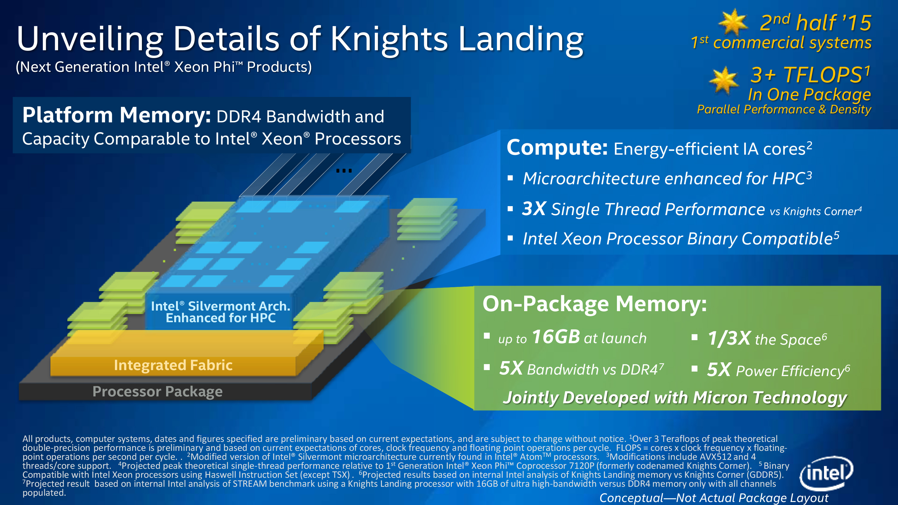
All told, Intel is planning on offering Knights Landing processors containing up to 72 of these cores, with double precision floating point (FP64) performance expected to exceed 3 TFLOPs. This will of course depend in part on Intel’s yields and clockspeeds – Knights Landing will be a 14nm part, a node whose first products won’t reach end-user hands until late this year – so while Knights Landing’s precise performance is up in the air, Intel is making it extremely clear that they are aiming very high.
Which brings us to this week and Intel’s latest batch of details. With last year focusing on the heart of the beast, Intel is spending ISC 2014 explaining how they intend to feed the beast. A processor that can move that much data is not going to be easy to feed, so Intel is going to be turning to some very cutting edge technologies to do it.
First and foremost, when it comes to memory Intel has found themselves up against a wall. With Knights Corner already using a very wide (512-bit) GDDR5 memory bus, Intel is in need of an even faster memory technology to replace GDDR5 for Knights Landing. To accomplish this, Intel and Micron have teamed up to bring a variant of Hybrid Memory Cube (HMC) technology to Knights Landing.

Hybrid Memory Cube (HMC)
Through the HMC Consortium, both Intel and Micron have been working on developing HMC as a next-generation memory technology. By stacking multiple DRAM dies on top of each other, connecting those dies to a controller at the bottom of the stack using Through Silicon Vias (TSVs), and then placing those stacks on-package with a processor, HMC is intended to greatly increase the amount of memory bandwidth that can be used to feed a processor. This is accomplished by putting said memory as close to the processor as possible to allow what’s essentially an extremely wide memory interface, through which an enormous amount of memory bandwidth can be created.
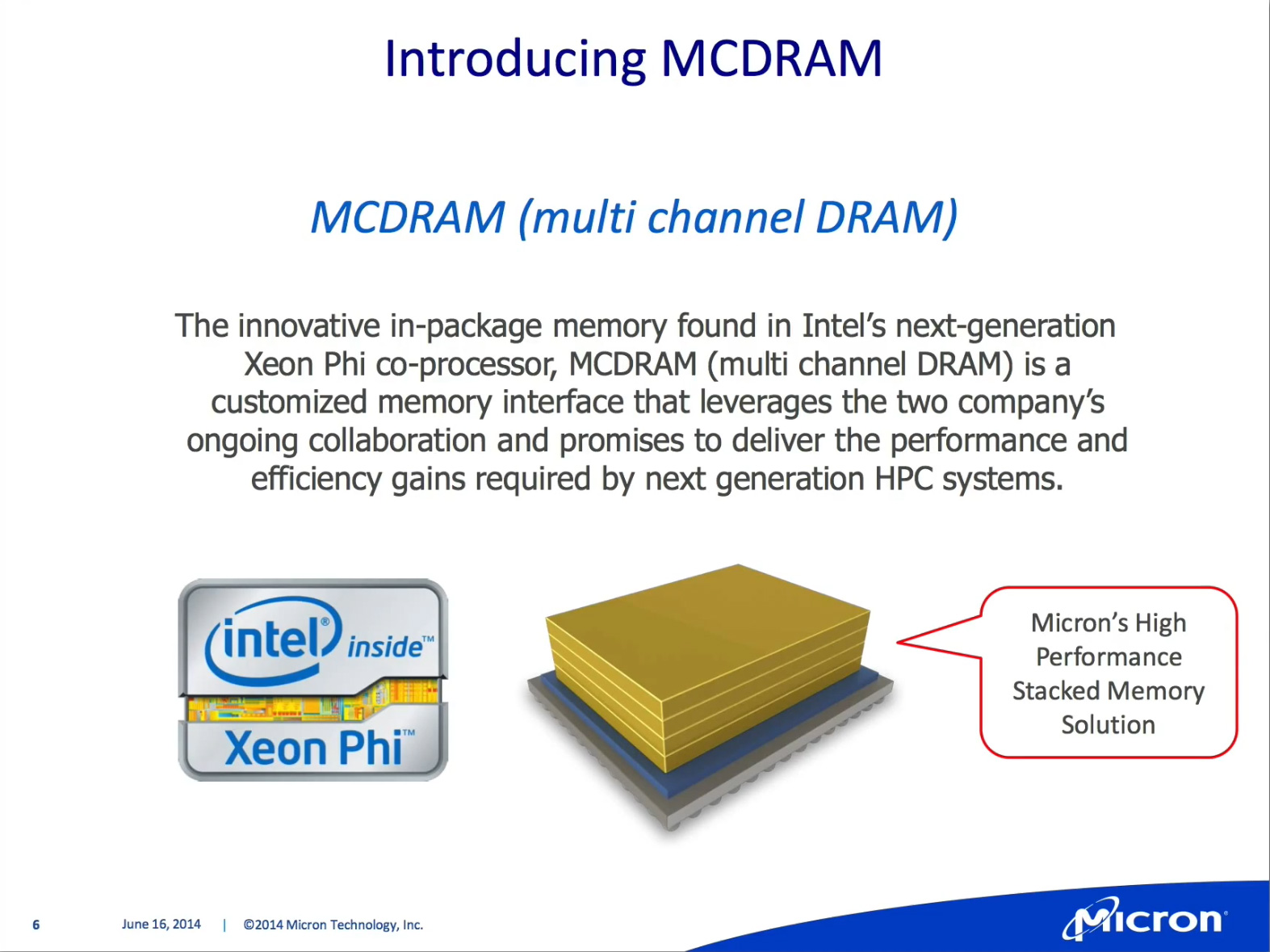
Image Courtesy InsideHPC.com
For Knights Landing, Intel and Micron will be using a variant of HMC designed just for Intel’s processor. Called Multi-Channel DRAM (MCDRAM), Intel and Micron have taken HMC and replaced the standard memory interface with a custom interface better suited for Knights Landing. The end result is a memory technology that can scale up to 16GB of RAM while offering up to 500GB/sec of memory bandwidth (nearly 50% more than Knights Corner’s GDDR5), with Micron providing the MCDRAM modules. Given all of Intel’s options for the 2015 time frame, the use of a stacked DRAM technology is among the most logical and certainly most expected (we've already seen NVIDIA plan to follow the same route with Pascal); however the use of a proprietary technology instead of HMC for Knights Landing comes as a surprise.
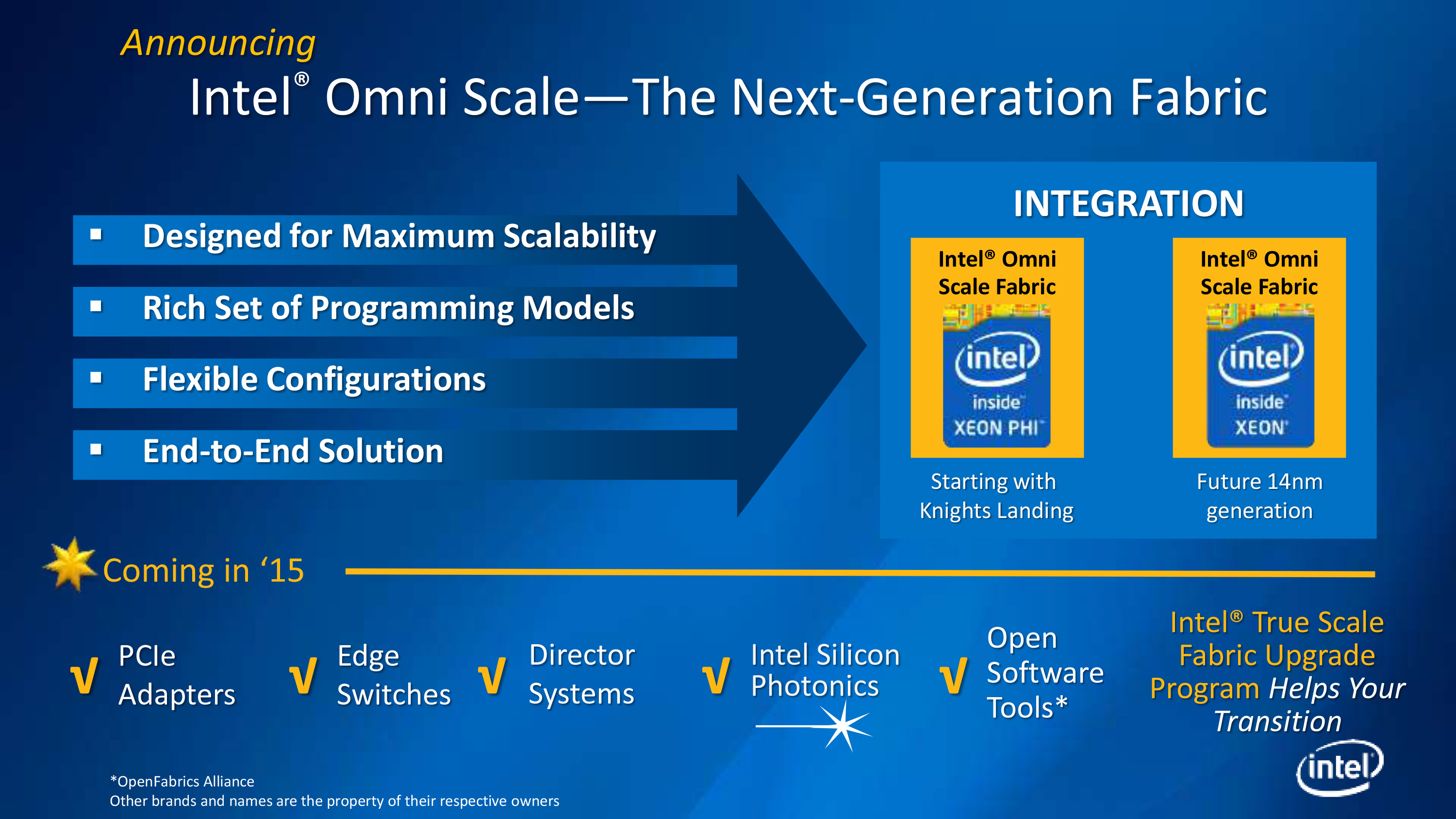
Moving on, while Micron’s MCDRAM solves the immediate problem of feeding Knights Landing, RAM is only half of the challenge Intel faces. The other half of the challenge for Intel is in HPC environments where multiple Knights Landing processors will be working together on a single task, in which case the bottleneck shifts to getting work to these systems. Intel already has a number of fabrics at hand to connect Xeon Phi systems, including their own True Scale Fabric technology, but like the memory situation Intel needs a much better solution than what they are using today.

For Knights Landing Intel will be using a two part solution. First and foremost, Intel will be integrating their fabric controller on to the Knights Landing processor itself, doing away with the external fabric controller, the space it occupies, and the potential bottlenecks that come from using a discrete fabric controller. The second part of Intel’s solution comes from developing a successor to True Scale Fabric – dubbed Omni Scale Fabric – to offer even better performance than Intel’s existing fabric solution. At this point Intel is being very tight lipped about the Omni Scale Fabric specifications and just how much of an improvement in inter-system communications Intel is aiming for, but we do know that it is part of a longer term plan. Eventually Intel intends to integrate Omni Scale Fabric controllers not just in to Knights Landing processors but traditional Xeon CPUs too, further coupling the two processors by allowing them to communicate directly through the fabric.
Last but not least however, thanks in large part to the consolidation offered by using MCDRAM, Intel is also going to be offering Knights Landing in a new form factor. Along with the traditional PCIe card form factor that Knights Corner is available in today, Knights Landing will also be available in a socketed form factor, allowing it to be installed alongside Xeon processors in appropriate motherboards. Again looking to remove any potential bottlenecks, by socketing Knights Landing Intel can directly connect it to other processors via Quick Path Interconnect as opposed to the slower PCI-Express interface. Furthermore by being socketed Knights Landing would inherit the Xeon processor’s current NUMA capabilities, sharing memory and memory spaces with Xeon processors and allowing them to work together on a workload heterogeneously, as opposed to Knights Landing operating as a semi-isolated device at the other end of a PCIe connection. Ultimately Intel is envisioning programs being written once and run across both types of processors, and with Knights Landing being binary compatible with Haswell, socketing Knights Landing is the other part of the equation that is needed to make Intel’s goals come to fruition.
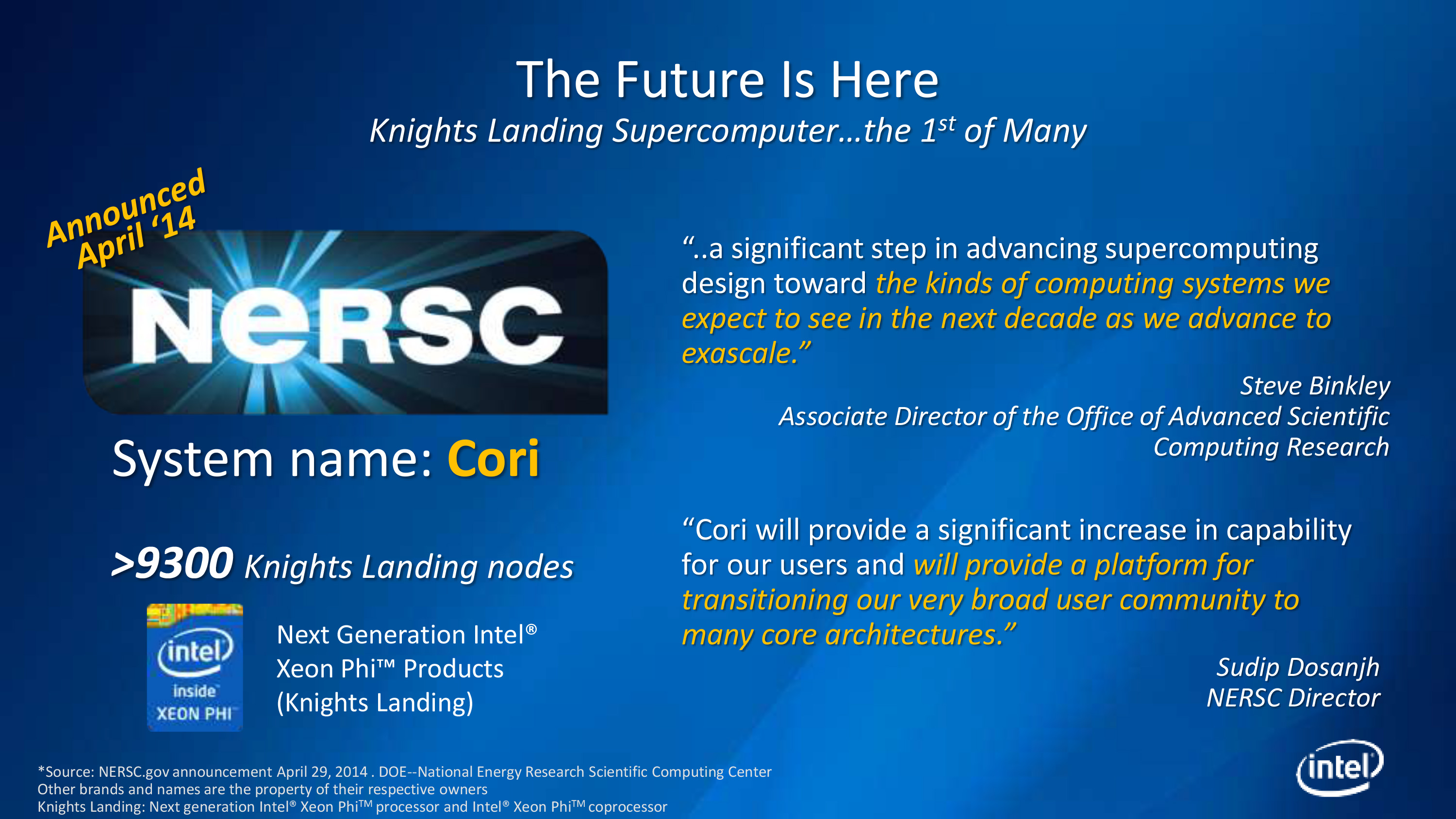
Wrapping things up, with this week’s announcements Intel is also announcing a launch window for Knights Landing. Intel is expecting to ship Knights Landing in H2’15 – roughly 12 to 18 months from now. In the meantime the company has already lined up its first Knights Landing supercomputer deal with the National Energy Research Scientific Computing Center, who will be powering their forthcoming Cori supercomputer with 9300 Knights Landing nodes. Intel currently enjoys being the CPU supplier for the bulk of the Top500 ranked supercomputers, and with co-processors becoming increasingly critical to these supercomputers Intel is shooting to become the co-processor vendor of choice too.
Source: Intel


41 Comments
View All Comments
makerofthegames - Friday, June 27, 2014 - link
No, Itanium failed because nobody could make a good compiler for it, including Intel. VLIW sucks for general-purpose computing. It works for a few workloads (graphics, mainly) but on anything relying on memory performance it's worthless.x86 decoding isn't hard - it's instruction reordering that takes up all that die space. Itanium tried to do all that at compile-time, which doesn't work because it needs to know which data is cached or not.
basroil - Monday, June 30, 2014 - link
VLIW has been around for a while, and you can make some ridiculously fast programs with it... In assembly. Even AMD dabbled with it in their 5000-6000 series GPUs, but yes, compiling generalized problems is a mess and why Intel positioned Itanium for infrastructure and application specific computing in recent yearstipoo - Thursday, June 26, 2014 - link
The Itanium business is still larger than all of AMD, hah. But yes, that didn't catch on so much that it was ready to replace x86, but that was going in the opposite direction as far as I know. Instead of reducing ISA complexity, it added some with even longer instructions. Intel is more limited going downwards to low power places rather than high power, the more you shrink cores to low power budgets the more that x86 ISA starts to look too large.dylan522p - Thursday, June 26, 2014 - link
Having more complicated instructions is beneficial in the long run especially when you break it into micro code. They can change how the microcode works with every generation as opposed to ARM or other CISC where they stay with the SAME instruction internally for years and years which bottlenecks performance. It helps somewhat with power, but as you scale up that is irrelevant.Homeles - Thursday, June 26, 2014 - link
ARM has an instruction decode block too. It's probably not terribly far off from an areal perspective, at a given level of performance. It may have been the case back in the 80s/90s, but the differences between RISC and CISC are much more nuanced now.RealWorldTech has an article from the year 2000 showing that while the differences between RISC and CISC had closed considerably, they still mattered. However, that was 14 years ago.
The ISA is basically meaningless today, in the context you're speaking of. The underlying architecture and its implementation is far, far more critical.
Take the Apple A7 vs. Intel's Silvermont. Despite being fairly close in performance, two Silvermont cores are significantly smaller than two Cyclone cores. The area difference worsens when you include the A7's L3 cache, which Silvermont designs do not rely on.
Even ARM to ARM comparisons can vary widely, even between custom implementations. The A7 is a dual core design that outpaces the quad core Krait 400. The area between the CPUs is fairly similar, although the A7 probably loses out by a small margin with the L3 cache included.
Back to RISC vs. CISC, The University of Wisconsin published a paper comparing the A9 vs. AMD's Bobcat and Intel's Saltwell Atom. Their conclusion: "Our study shows that RISC and CISC ISA traits are irrelevant to power and performance characteristics of modern cores."
http://research.cs.wisc.edu/vertical/papers/2013/h...
There's no doubt RISC had a considerable lead over CISC, but that was decades ago.
tabascosauz - Thursday, June 26, 2014 - link
True. I too am sick and tired of hearing the mentioning of ARM as this huge, inevitable looming monster on the horizon for Intel and proponents of x86. It isn't. Saying that Krait 400 = Cortex-A15 and Cyclone = A57 is like placing Bulldozer beside K10 and making direct comparisons. The different implementations of ARMv7 and ARMv8 in the ARM world are wholly different entities in terms of CPU and cache design.abufrejoval - Thursday, June 26, 2014 - link
I believe you have a rather valid point there: Creating a massively parallel SIMD enhanced general purpose CPU to compete with GPU was certainly a valid exercise, because it could be productive and effective on a far wider range of problems, a far wider existing code base and a far wider population of programmers.With ARM64 (or MIPS or any other new/cleaen 64-bit CPU design for that matter) more silicon real-estate might be used to create additional cores. How much or how many and how relevant that would be vs. the die area used for caches I don't know. Perhaps yields could be improved, because smaller complex logic core size means perhaps more cores for the same compute power but less is lost for a defect.
What I could not gauge is how the code using these SIMD AVX-512F instructions would actually be written or coded these days: x86/AVX-512F assembler won't easily convert to similar AVX-512F instructions on ARM64, but high level language code just might--with the right compiler.
Because Intel doesn't just do the CPU but (I believe) provides compilers and libraries around them, they most likely have a lead of a couple of years against any direct ARM competition.
But these days it's become far too easy to add and use FPGA or other special function IP blocks on ARM SoCs and all of a sudden Intel might potentially find itself in an arena with far more "knights" they ever imagined.
They can't quite escape the fact that any fixed workload on a general purpose architecture can be outperformed by a specific purpose one. More than ever chips aren't "best" or "better" but their quality or fitness depends on the mix of problems they are used for.
Kevin G - Friday, June 27, 2014 - link
The thing with ARM is that some instructions in earlier iterations (I'd have to check ARMv8) that don't need to be decoded at all. That's where mainly the RISC vs. CISC differences come into play today: die size. The area savings by having a simpler decoder In the case of Knight's Landing, how many cores could be added if the decoder was half its current size? 80 instead of 72?That's the problem that Intel is currently facing. Intel isn't using their high IPC cores but ones typical found in Atom. ARM designs can reach similar levels of IPC but potentially at a smaller die area. Thus even if Silvermont wins on IPC the competing RISC based SoC's could still have higher throughput due to more cores.
Intel does have an ace up their sleeve by having their own fabs. This enables them to produce larger dies and maintain similar raw areas for CPU's by having a fab process advantage. However, the fab process advantage is not going to be long lived due to the difficulties of future shrinks.
Vlad_Da_Great - Thursday, July 23, 2015 - link
@Kevin G. Not only that, chemical processes and material processes restrictions. Also the biggest advantage for INTC will always be, Design and FAB in one house. ARM minions will have to rely on "others" and in many occasions that will not work.Vlad_Da_Great - Thursday, July 23, 2015 - link
* material properties