Intel’s "Knights Landing" Xeon Phi Coprocessor Detailed
by Ryan Smith on June 26, 2014 10:00 AM ESTContinuing our ISC 2014 news announcements for the week, next up is Intel. Intel has taken to ISC to announce further details about the company’s forthcoming Knights Landing processor, the next generation of Intel’s Xeon Phi processors.
While Knights Landing in and of itself is not a new announcement – Intel has initially announced it last year – Intel has offered very few details on the makeup of the processor until now. However with Knights Landing scheduled to ship in roughly a year from now, Intel is ready to offer up further details about the processor and the capabilities.
As previously announced, as the successor to Intel’s existing Knights Corner (1st generation Xeon Phi), Knights Landing makes the jump from using Intel’s enhanced Pentium 1 (P54C) x86 cores to using the company’s modern Silvermont x86 cores, which currently lie at the heart of the Intel’s Atom processors. These Silvermont cores are far more capable than the older P54C cores and should significantly improve Intel’s single threaded performance. All the while these cores are further modified to incorporate AVX units, allowing AVX-512F operations that provide the bulk Knights Landing’s computing power and are a similarly potent upgrade over Knights Corner’s more basic 512-bit SIMD units.
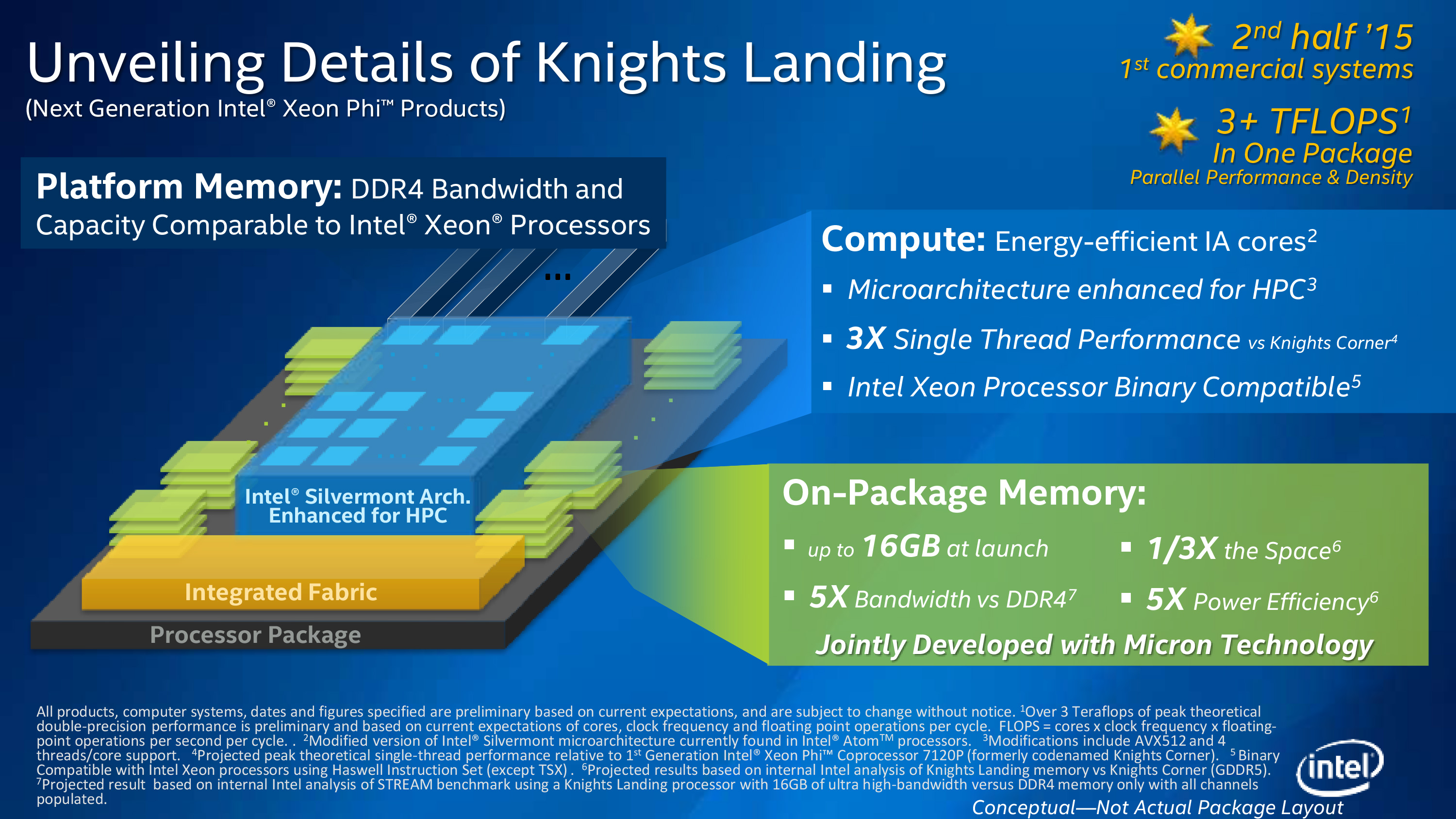
All told, Intel is planning on offering Knights Landing processors containing up to 72 of these cores, with double precision floating point (FP64) performance expected to exceed 3 TFLOPs. This will of course depend in part on Intel’s yields and clockspeeds – Knights Landing will be a 14nm part, a node whose first products won’t reach end-user hands until late this year – so while Knights Landing’s precise performance is up in the air, Intel is making it extremely clear that they are aiming very high.
Which brings us to this week and Intel’s latest batch of details. With last year focusing on the heart of the beast, Intel is spending ISC 2014 explaining how they intend to feed the beast. A processor that can move that much data is not going to be easy to feed, so Intel is going to be turning to some very cutting edge technologies to do it.
First and foremost, when it comes to memory Intel has found themselves up against a wall. With Knights Corner already using a very wide (512-bit) GDDR5 memory bus, Intel is in need of an even faster memory technology to replace GDDR5 for Knights Landing. To accomplish this, Intel and Micron have teamed up to bring a variant of Hybrid Memory Cube (HMC) technology to Knights Landing.

Hybrid Memory Cube (HMC)
Through the HMC Consortium, both Intel and Micron have been working on developing HMC as a next-generation memory technology. By stacking multiple DRAM dies on top of each other, connecting those dies to a controller at the bottom of the stack using Through Silicon Vias (TSVs), and then placing those stacks on-package with a processor, HMC is intended to greatly increase the amount of memory bandwidth that can be used to feed a processor. This is accomplished by putting said memory as close to the processor as possible to allow what’s essentially an extremely wide memory interface, through which an enormous amount of memory bandwidth can be created.
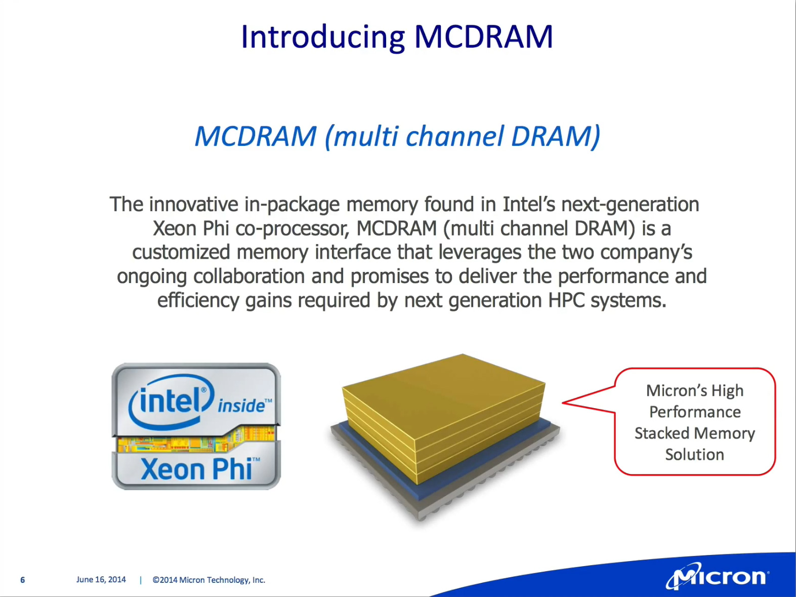
Image Courtesy InsideHPC.com
For Knights Landing, Intel and Micron will be using a variant of HMC designed just for Intel’s processor. Called Multi-Channel DRAM (MCDRAM), Intel and Micron have taken HMC and replaced the standard memory interface with a custom interface better suited for Knights Landing. The end result is a memory technology that can scale up to 16GB of RAM while offering up to 500GB/sec of memory bandwidth (nearly 50% more than Knights Corner’s GDDR5), with Micron providing the MCDRAM modules. Given all of Intel’s options for the 2015 time frame, the use of a stacked DRAM technology is among the most logical and certainly most expected (we've already seen NVIDIA plan to follow the same route with Pascal); however the use of a proprietary technology instead of HMC for Knights Landing comes as a surprise.
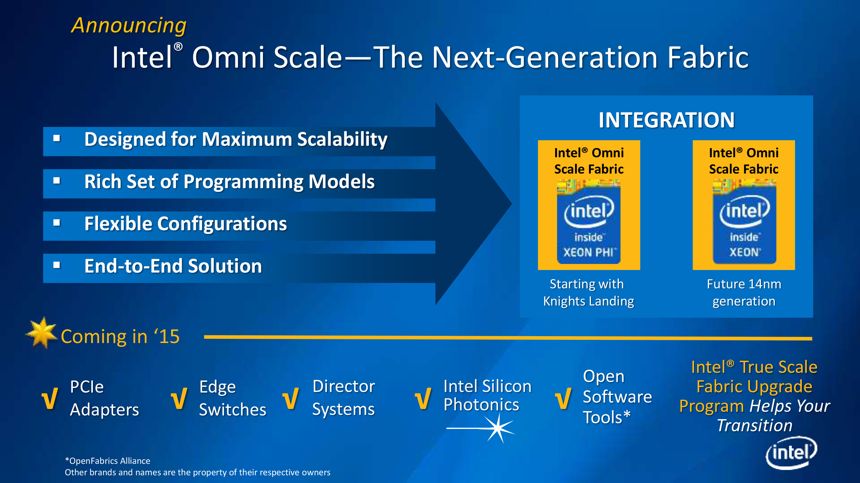
Moving on, while Micron’s MCDRAM solves the immediate problem of feeding Knights Landing, RAM is only half of the challenge Intel faces. The other half of the challenge for Intel is in HPC environments where multiple Knights Landing processors will be working together on a single task, in which case the bottleneck shifts to getting work to these systems. Intel already has a number of fabrics at hand to connect Xeon Phi systems, including their own True Scale Fabric technology, but like the memory situation Intel needs a much better solution than what they are using today.

For Knights Landing Intel will be using a two part solution. First and foremost, Intel will be integrating their fabric controller on to the Knights Landing processor itself, doing away with the external fabric controller, the space it occupies, and the potential bottlenecks that come from using a discrete fabric controller. The second part of Intel’s solution comes from developing a successor to True Scale Fabric – dubbed Omni Scale Fabric – to offer even better performance than Intel’s existing fabric solution. At this point Intel is being very tight lipped about the Omni Scale Fabric specifications and just how much of an improvement in inter-system communications Intel is aiming for, but we do know that it is part of a longer term plan. Eventually Intel intends to integrate Omni Scale Fabric controllers not just in to Knights Landing processors but traditional Xeon CPUs too, further coupling the two processors by allowing them to communicate directly through the fabric.
Last but not least however, thanks in large part to the consolidation offered by using MCDRAM, Intel is also going to be offering Knights Landing in a new form factor. Along with the traditional PCIe card form factor that Knights Corner is available in today, Knights Landing will also be available in a socketed form factor, allowing it to be installed alongside Xeon processors in appropriate motherboards. Again looking to remove any potential bottlenecks, by socketing Knights Landing Intel can directly connect it to other processors via Quick Path Interconnect as opposed to the slower PCI-Express interface. Furthermore by being socketed Knights Landing would inherit the Xeon processor’s current NUMA capabilities, sharing memory and memory spaces with Xeon processors and allowing them to work together on a workload heterogeneously, as opposed to Knights Landing operating as a semi-isolated device at the other end of a PCIe connection. Ultimately Intel is envisioning programs being written once and run across both types of processors, and with Knights Landing being binary compatible with Haswell, socketing Knights Landing is the other part of the equation that is needed to make Intel’s goals come to fruition.
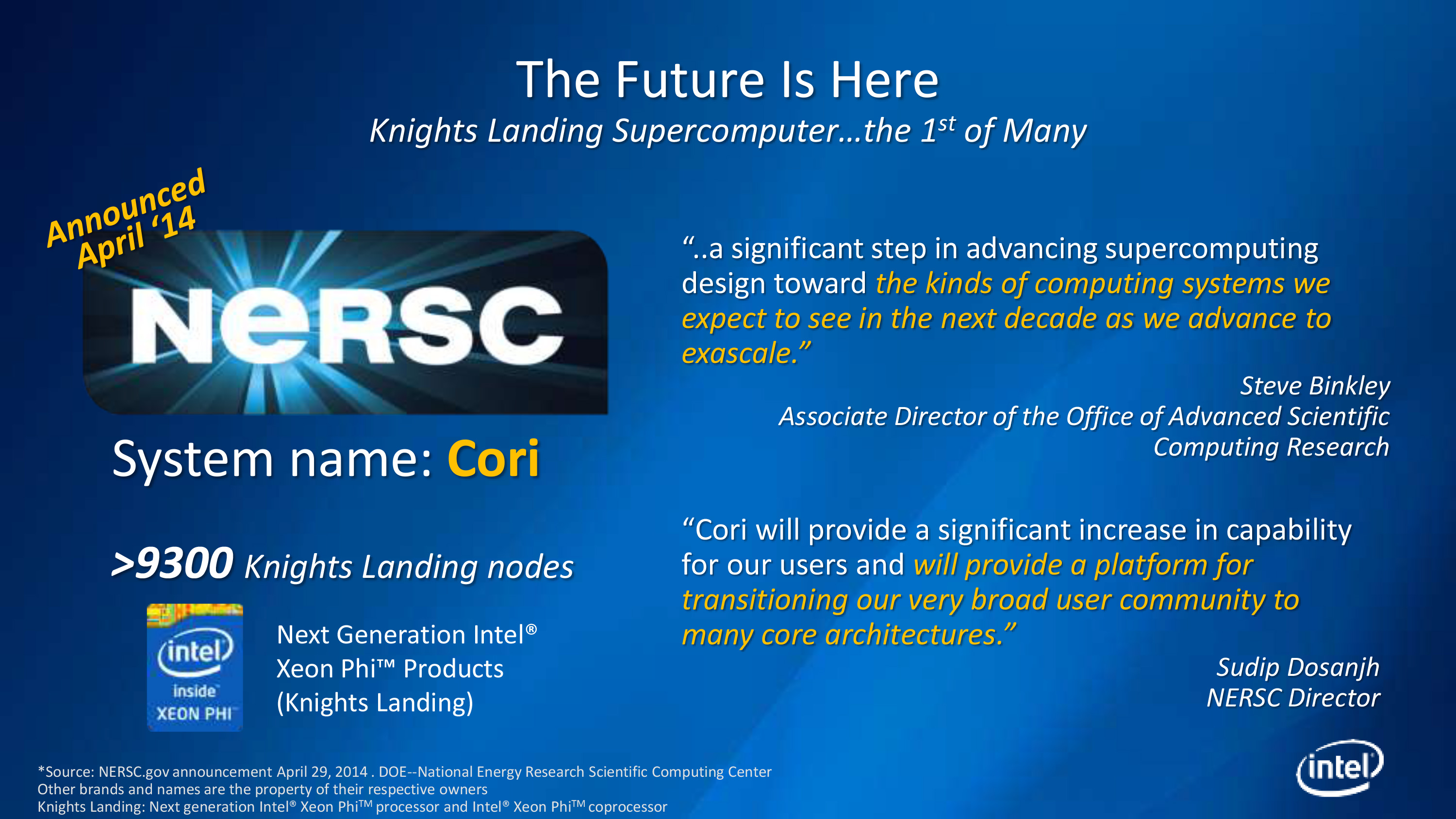
Wrapping things up, with this week’s announcements Intel is also announcing a launch window for Knights Landing. Intel is expecting to ship Knights Landing in H2’15 – roughly 12 to 18 months from now. In the meantime the company has already lined up its first Knights Landing supercomputer deal with the National Energy Research Scientific Computing Center, who will be powering their forthcoming Cori supercomputer with 9300 Knights Landing nodes. Intel currently enjoys being the CPU supplier for the bulk of the Top500 ranked supercomputers, and with co-processors becoming increasingly critical to these supercomputers Intel is shooting to become the co-processor vendor of choice too.
Source: Intel


41 Comments
View All Comments
ravyne - Monday, July 7, 2014 - link
x86/x64 ISA compatibility really isn't the problem -- you could make the argument that these ISAs are large, and kind of ugly -- but its affect on die-size is minimal. In fact, only between 1-2 percent of your CPU is actually doing direct computation -- and nearly all the rest of the complexity is wiring or latency-hiding mechanisms (OoO execution engines, SMT, buffers, caches). Silvermont, IIRC, is something of a more-direct x86/x64 implementation than is typical though (others translate all x86/x64 ISA to an internal RISC-like ISA), so its hard to say, but I think in general these days that ISA has very little impact on die size, performance, or power draw -- regardless of vendor or ISA, there's a fairly linear scale relating process-size, die-size, power consumption, and performance.Madpacket - Thursday, June 26, 2014 - link
Looks impressive. Now only if we could have a generous amount of stacked DRAM to sit alongside a new APU we could gain respectable gaming speeds.nathanddrews - Thursday, June 26, 2014 - link
Mass quantities of fast DRAM... McDRAM is the perfect name.Homeles - Thursday, June 26, 2014 - link
Clever :-)Homeles - Thursday, June 26, 2014 - link
You'll undoubtedly see it, but the question is when. Stacked DRAM won't be debuting in consumer products until late this year at the earliest. AMD will likely be the first to market, with their partnership with Hynix for HBM. There was a chance Intel would put Xeon Phi out first, but with a launch in the second half of 2015, that's pretty much erased.Still, initial applications will be for higher margin parts, like this Xeon Phi, and AMD's higher-end GPUs. It will be some time before costs come down to be used in the more cost-sensitive APU segment.
abufrejoval - Thursday, June 26, 2014 - link
Well a slightly different type of stacked DRAM is already in wide use on consumer devices today: My Samsung Galaxy Note uses a nice stack of six dies mounted on top of the CPU.It's using BGA connections rather than silicon through vias, so it's not quite the same.
What I don't know (and would love to know) is whether that BGA stacking allows Samsung to maintain CMOS logic between the DRAM chips or whether they need to switch to "TTL like" signals and amplifiers already.
If I don't completely misunderstand this ability to maintain CMOS levels and signalling across dice would be one of the critical differentiators for silicon vias.
But while stacked DRAM (of both types) may work ok on smartphone SoCs not exceeding 5 Watt of power dissipation I can't help but imagine that with ~100Watts of Knights Landing power consumption below, stacked DRAM on top may add significant cooling challenges.
Perhaps these silicon through vias will be coupled with massive copper (cooling) towers going through the entire stack of CPU and DRAM dice, but again that seems to entail quite a few production and packaging challenges!
Say you have 10x10 cooling towers across the chip stack: Just imagine the cost of a broken drill on hole #99.
I guess actually thermally optimized BGA interconnects may be easier to manage overall, but at 100Watts?
I can certainly see how this won't be ready tomorrow and not because it's difficult to do the chips themselves.
Putting that stack together is an entirely new ball game (grid or not ;-) and while a solution might never pay for itself in the Knights Corner ecosystem, that tech in general would fit on anything else Intel does produce.
My bet: They won't actually put the stacked DRAM on top of the CPU but go for a die carrier solution very much like the eDRAM on Iris Pro.
iceman-sven - Thursday, June 26, 2014 - link
This might hint a faster Skylake-ep/-ex release. EP could be moved from late 3Q17 to late 4Q16. Even skip Broadwell-EP.I hope so.
iceman-sven - Thursday, June 26, 2014 - link
I mean from late 3Q16 to late 4Q15Why no edit. Dammit.
Pork@III - Thursday, June 26, 2014 - link
Just silicon, it make no troubles on me.tuxRoller - Thursday, June 26, 2014 - link
So, what's the flops/W?