GDDR5X Standard Finalized by JEDEC: New Graphics Memory up to 14 Gbps
by Anton Shilov on January 22, 2016 3:00 PM EST
In Q4 2015, JEDEC (a major semiconductor engineering trade organization that sets standards for dynamic random access memory, or DRAM) finalized the GDDR5X specification, with accompianing white papers. This is the memory specification which is expected to be used for next-generation graphics cards and other devices. The new technology is designed to improve bandwidth available to high-performance graphics processing units without fundamentally changing the memory architecture of graphics cards or memory technology itself, similar to other generations of GDDR, although these new specifications are arguably pushing the phyiscal limits of the technology and hardware in its current form.
The GDDR5X SGRAM (synchronous graphics random access memory) standard is based on the GDDR5 technology introduced in 2007 and first used in 2008. The GDDR5X standard brings three key improvements to the well-established GDDR5: it increases data-rates by up to a factor of two, it improves energy efficiency of high-end memory, and it defines new capacities of memory chips to enable denser memory configurations of add-in graphics boards or other devices. What is very important for developers of chips and makers of graphics cards is that the GDDR5X should not require drastic changes to designs of graphics cards, and the general feature-set of GDDR5 remains unchanged (and hence why it is not being called GDDR6).
Performance Improvements
Nowadays highly binned GDDR5 memory chips can operate at 7 Gbps to 8 Gbps data rates. While it is possible to increase performance of the GDDR5 interface for command, address and data in general, according to Micron Technology, one of the key designers of GDDR5X, there are limitations when it comes to array speed and command/address protocols. In a bid to improve performance of the GDDR5 memory, engineers had to change internal architecture of memory chips significantly.
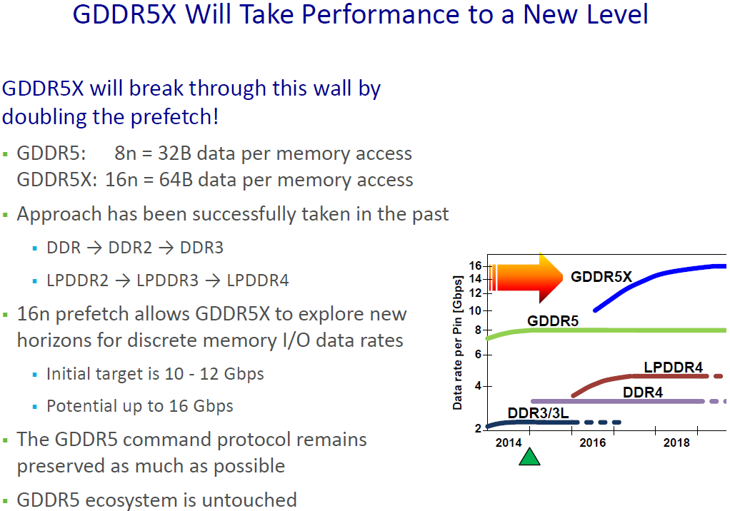
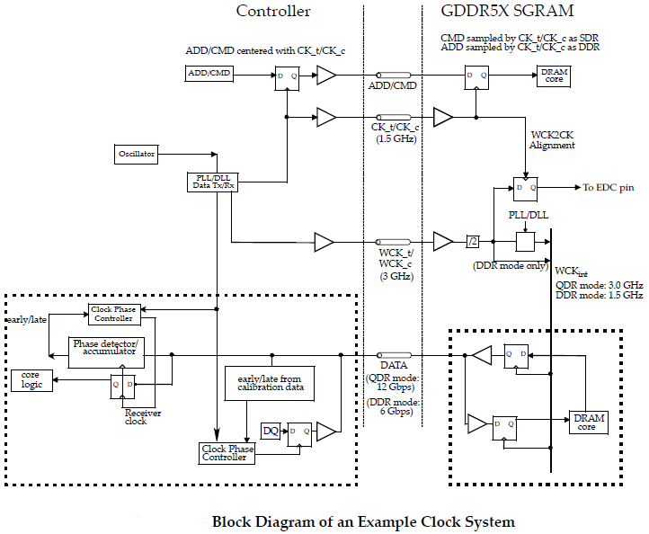
The key improvement of the GDDR5X standard compared to the predecessor is its all-new 16n prefetch architecture, which enables up to 512 bit (64 Bytes) per array read or write access. By contrast, the GDDR5 technology features 8n prefetch architecture and can read or write up to 256 bit (32 Bytes) of data per cycle. Doubled prefetch and increased data transfer rates are expected to double effective memory bandwidth of GDDR5X sub-systems. However, actual performance of graphics cards will depend not just on DRAM architecture and frequencies, but also on memory controllers and applications. Therefore, we will need to test actual hardware to find out actual real-world benefits of the new memory.
Just like the predecessor, GDDR5X functions with two different clock types - a differential command clock (CK) to where address and command inputs are referenced, as well as a forwarded differential write clock (WCK) where read and write data are referenced to. WCK runs at a frequency that is two times higher than the CK. The data can be transmitted at double data rate (DDR) or quad data rate (QDR) relative to the differential write clock (WCK), depending whether 8n prefetch or 16n prefetch architecture and protocols are used. Accordingly, if makers of chips manage to increase CK clock to 1.5 GHz, then data rate in QDR/16n mode will rise to 12 Gbps.
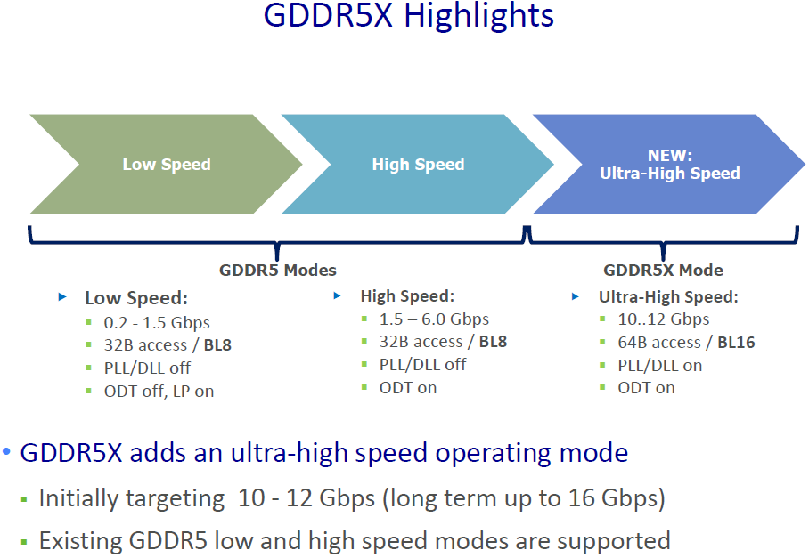
Since the GDDR5X protocol and interface training sequence are similar to those of the GDDR5, it should be relatively easy for developers of chips to adjust their memory controllers to the new type of memory. However, since the QDR mode (which is called Ultra High Speed mode in Micron’s materials) mandates usage of PLLs/DLLs (Phase Locked Loops, Delay Locked Loops), there will be certain design changes to design of high-end memory chips.
JEDEC’s GDDR5X SGRAM announcement discusses data rates from 10 to 14 Gbps, but Micron believes that eventually they could be increased to 16 Gbps. It is hard to say whether commercial chips will actually hit such data rates, keeping in mind that there are new types of memory incoming. However, even a 256-bit GDDR5X memory sub-systems running at 14 Gbps could provide up to 448 GBps of memory bandwidth, just 12.5% lower compared to that of AMD’s Radeon R9 Fury X (which uses first-gen HBM).
| GPU Memory Math | |||||||||
| AMD Radeon R9-290X |
NVIDIA GeForce GTX 980 Ti |
NVIDIA GeForce GTX 960 |
AMD Radeon R9 Fury X |
Samsung's 4-Stack HBM2 based on 8 Gb DRAM | Theoretical GDDR5X 256-bit sub-system |
Theoretical GDDR5X 128-bit sub-system |
|||
| Total Capacity | 4 GB | 6 GB | 2 GB | 4 GB | 16 GB | 8 GB | 4 GB | ||
| B/W Per Pin | 5 Gb/s | 7 Gb/s | 7 Gb/s | 1 Gb/s | 2 Gb/s | 14 Gb/s | 14 Gb/s | ||
| Chip capacity | 2 Gb | 4 Gb | 4 Gb | 1 GB | 4 GB | 1 GB (8 Gb) |
1 GB (8 Gb) |
||
| No. Chips/Stacks | 16 | 12 | 4 | 4 | 4 | 8 | 4 | ||
| B/W Per Chip/Stack | 20 GB/s |
28 GB/s |
28 GB/s |
128 GB/s |
256 GB/s |
56 GB/s |
56 GB/s |
||
| Bus Width | 512-bit | 384-bit | 128-bit | 4096-bit | 4096-bit | 256-bit | 128-bit | ||
| Total B/W | 320 GB/s |
336 GB/s |
112 GB/s |
512 GB/s |
1 TB/s |
448 GB/s |
224 GB/s |
||
| Estimated DRAM Power Consumption |
30 W | 31.5 W | 10 W | 14.6 W | n/a | 20 W | 10 W | ||
Capacity Improvements
Performance was not the only thing that developers of the GDDR5X had to address. Many applications require not only high-performance memory, but a lot of high-performance memory. Increased capacities of GDDR5X chips will enable their adoption by broader sets of devices in addition to graphics/compute cards, game consoles and network equipment as well as other areas. Initially one would expect the high density configurations to be slightly conservative on frequency to begin with.
The GDDR5 standard covered memory chips with 512 Mb, 1 Gb, 2 Gb, 4 Gb and 8 Gb capacities. The GDDR5X standard defines devices with 4 Gb, 6 Gb, 8 Gb, 12 Gb and 16 Gb capacities. Typically, mainstream DRAM industry tends to double capacities of memory chips because of economic and technological reasons. However, with GDDR5X the industry decided to ratify SGRAM configurations with rather unusual capacities — 6Gb and 12Gb.
The mobile industry already uses LPDDR devices with 3 Gb, 6 Gb and 12 Gb capacities in a bid to maximize flexibility of memory configurations for portable electronics. As it appears, companies developing standards for graphics DRAM also wanted to capitalize on flexibility. A GDDR5X chip with 16 Gb capacity made using 20 nm or 16/18 nm process technology would have a rather large die size and thus high cost. However, the size and cost of a 12 Gb DRAM IC should be considerably lower and such a chip could arguably address broader market segments purely on cost.
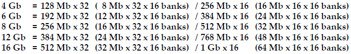
Just like in case of the GDDR5, the GDDR5X standard fully supports clamshell mode, which allows two 32-bit memory chips to be driven by one 32-bit memory controller by sharing address and command bus while reducing the number of DRAM IC’s I/Os to 16. Such operation has no impact on system bandwidth, but allows doubling the amount of memory components per channel. For example, it should be theoretically possible to build a graphics card with 64 GB of GDDR5X using one GPU with a 512-bit memory bus as well as 32 16 Gb GDDR5X memory chips.
Unusual capacities will help GDDR5X to better address all market segments, including graphics cards, HPC (high performance computing), game consoles, network equipment and so on. However, it should be noted that the GDDR5X has extremely potent rival, the second-gen HBM, which offers a number of advantages, especially in the high-end segment of the graphics and HPC markets.
Energy Efficiency
Power consumption and heat dissipation are two major limiting factors of compute performance nowadays. When developing the GDDR5X standard, the industry implemented a number of ways to keep power consumption of the new graphics DRAM in check.
Supply voltage and I/O voltages of the GDDR5X were decreased from 1.5V on today’s high-end GDDR5 memory devices to 1.35V. Reduction of Vdd and Vddq should help to cut power consumption of the new memory by up to 10%, which is important for high-performance and mobile devices where the memory can take a sizable chunk of the available power budget.
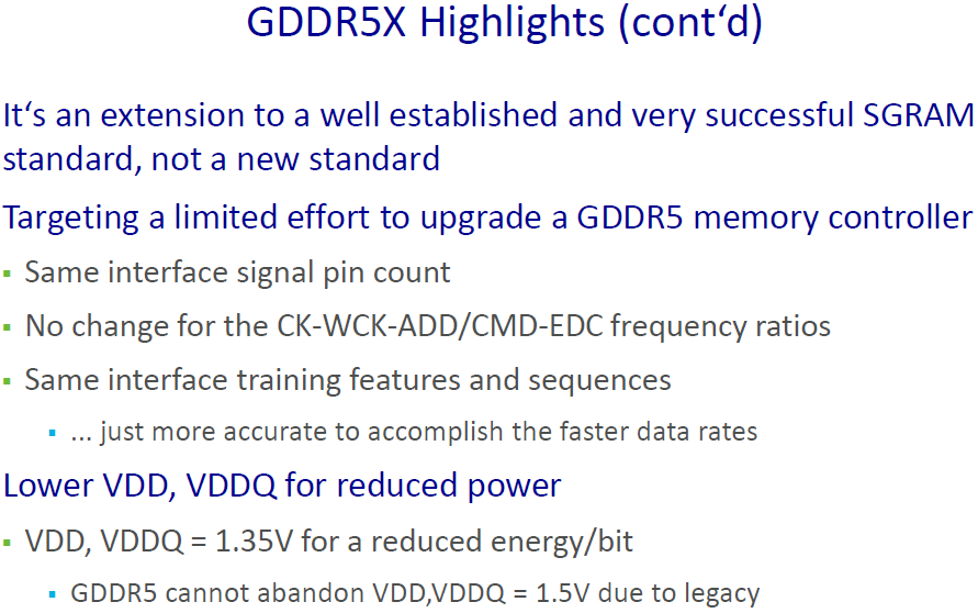
The reduction of supply and I/O voltages is not the only measure to cut power consumption of the new memory. The GDDR5X standard makes temperature sensor controlled refresh rate a compulsory feature of the technology, something that could help to optimize power consumption in certain scenarios. Moreover, there are a number of other features and commands, such as per-bank self refresh, hibernate self refresh, partial array self refresh and other, that were designed to shrink the energy consumption of the new SGRAM.
Due to lower voltages and a set of new features, power consumption of a GDDR5X chip should be lower compared to that of a GDDR5 chip at the same clock-rates. However, if we talk about target data rates of the GDDR5X, then power consumption of the new memory should be similar or slightly higher than that of GDDR5, according to Micron. The company says that GDDR5X’s power consumption is 2-2.5W per DRAM component and 10-30W per board. Even with similar/slightly higher power consumption compared to the GDDR5, the GDDR5X is being listed as considerably more energy efficient due to its improved theoretical performance.
We do not know specifications of next-generation graphics adapters (for desktops and laptops) from AMD and NVIDIA, but if developers of GPUs and DRAMs can actually hit 14 Gb/s data-rates with GDDR5X memory, they will double the bandwidth available to graphics processors vs GDDR5 without significantly increasing power consumption. Eventually, more efficient data-rates and unusual capacities of the GDDR5X could help to actually decrease power consumption of certain memory sub-systems.
Implementation
While internally a GDDR5X chip is different from a GDDR5 one, the transition of the industry to GDDR5X is a less radical step than the upcoming transition to the HBM (high-bandwidth memory) DRAM. Moreover, even the transition from the GDDR3/GDDR4 to the GDDR5 years ago was considerably harder than transition to the GDDR5X is going to be in the coming years.
The GDDR5X-compliant memory chips will come in 190-ball grid array packaging (as compared to 170-ball packaging used for current GDDR5), thus, they will not be pin-to-pin compatible with existing GDDR5 ICs or PCBs for modern graphics cards. But while the GDDR5X will require development of new PCBs and upgrades to memory controllers, everything else works exactly like in case of the GDDR5: the interface signal training features and sequences are the same, error detection is similar, protocols have a lot of resemblances, even existing GDDR5 low and high speed modes are supported to enable mainstream and low-power applications. BGA packages are inexpensive, and they do not need silicon interposers nor use die-stacking techniques which HBM requires.
Implementation of GDDR5X should not be too expensive both from R&D and production perspectives; at least, this is something that Micron implied several months ago when it revealed the first details about the technology.
Industry Support
The GDDR5X is a JEDEC standard supported by its members. The JEDEC’s document covering the technology contains vendor IDs for three major DRAM manufacturers: Micron, Samsung and SK Hynix. Identification of the memory producers are needed for controllers to to differentiate between various vendors and different devices, and listing the memory makers demonstrates that they participated in development, considered features and balloted on them at JEDEC’s meetings, which may indicate their interest in supporting the technology. Unfortunately, exact plans for each of the companies regarding GDDR5X production are unknown, though we would expect GDDR5X parts to fit between the current GDDR5 high end and anything implementing HBM, or for implementing higher memory capacity on lower end GPUs. Micron plans to start mass production of its GDDR5X memory chips in mid-2016, so we might see actual GDDR5X-based memory sub-systems in less than six months from now.
NVIDIA, currently the world’s largest supplier of discrete graphics processors, said that that as a member of JEDEC it participates in the development of industry standards like GDDR5X. AMD is also a member of JEDEC and it usually plays a key role in development of memory standards. Both of these companies also employ compression algorithms to allieviate the stress on texture transfers between the GPU and memory, and thus an increase in bandwidth (as shown by Fiji) plus an increase in density can see benefits in texture rich or memory bound compute scenarios.
While specific plans of various companies regarding the GDDR5X are unclear, the technology has a great potential if the numbers are accurate (it has to be, it's a standard) and has all chances to be adopted by the industry. The main rival of the GDDR5X, second-generation HBM, can offer higher bandwidth, lower power consumption and smaller form-factors, but at the cost of design and manufacturing complexities. In fact, what remains to be seen is whether the HBM and the GDDR5X will actually compete directly against each other or will just become two complementary types of memory. Different applications nowadays have different requirements, and an HBM memory sub-system with 1 TBps of bandwidth makes a perfect sense for a high-end graphics adapter. However mainstream video cards should work perfectly with GDDR5X, and chances are we will see both in play at different market focal points.
Source: JEDEC


70 Comments
View All Comments
BurntMyBacon - Monday, January 25, 2016 - link
@Yojimbo: "GDDR5 has been used for 7 1/2 years, not 10. 28nm graphics cards came out 4 years ago, not 6. Why do you exaggerate instead of using the real numbers?"I don't think Samus was exaggerating. Rather, Samus was simply trying to make a point and didn't feel the need to spend the time to get exact numbers for a fairly well know fact that the industry has been held up as a whole by lack of process improvements that will be present in the next gen graphics chips. I'm sure Samus thought the estimates thrown out, while not precise would be close enough to get the point across. To be fair, while they were off the mark, the point of the post still stands:
@Samus: "HBM requires entirely new memory controllers, generally graphics chips need to be built from the ground up to support it, and considering its cost and capacity restrictions per block (even HBM2) I suspect GDDR5X will be the industry standard for the next few years."
rarson - Friday, January 29, 2016 - link
A huge advantage of HDM over GDDR5 is packaging. Even if performance of GDDR5X were similar to HBM 1, the same capacity memory will take up a lot more PCB space. Easily demonstrated by the Fury cards, which are tiny compared to other GDDR5 cards.Personally, I don't see how GDDR5X has any hope of competing with HBM (especially HBM 2) in the high-end graphics card market, but GDDR5X, if it's cheap enough, could be a decent replacement for lower end cards that like to use DDR3, or better yet, a faster replacement for main system RAM. That's what I'd like to see: GDDR5X on the motherboard, and HBM 2 on the graphics card. In large quantities of both, please.
Despoiler - Monday, January 25, 2016 - link
HBM actually doesn't require new memory controllers in the sense that you are presenting. If you knew what you were talking about you'd know that the memory controller is the logic slice that is part of the HBM stack. ie it's off the GPU die. The GPU die only contains a PHY.Your argument that HBM was created primarily for bandwidth is incorrect. HBM was primarily created because GDDR is hitting a power wall. The clock speeds are so high that the power budget is too much to maintain. Clock speeds also are not infinite. We are at that wall also. HBM solves those issue for many years to come.
Also, 20nm? That got skipped. 14/16nm is what AMD and Nvidia are using. Don't even try to say they are close enough so we should "read between the lines."
xenol - Tuesday, January 26, 2016 - link
My guess is GDDR memory is going to be around for a while to supply the lower end GPUs or other areas where it may not make sense to use HBM for some reason or another.DanNeely - Friday, January 22, 2016 - link
Agreed. It looks really promising as a bridge tech for use in more price sensitive market segments where the cost of the interposer needed for HBM would be prohibitive. With time I suspect the interposer costs will drop; both because the tech itself becomes more mature and because they can be made on older processes that will get steadily cheaper due to lack of general demand.For this year's card I suspect the $30 pricepoint that's been floated for the first generation ones AMDs using now will probably mean most cards at the sub $200 pricepoint will continue to use conventional GDDR of some sort. There'll probably be some exceptions (especially if smaller/cheaper interposers are available for 1/2 stack implementations); but compact/low profile variant cards have never been a big segment of the market due to both the extra cost involved and the poorer cooling from smaller heatsinks and less fans.
extide - Friday, January 22, 2016 - link
Yeah I don't think we will see HBM cards anywhere NEAR the $200 price point, at least this gen. My bet is that we will see one GPU from AMD with HBM. Then nVidia will be one or two, GP100 for sure, GP104, maybe. Then the next cards down will be GDDR5X, and then below that DDR3/4, for the ultra cheap oem stuff. I bet we will see GDDR5 phased out pretty quick.DanNeely - Saturday, January 23, 2016 - link
I could've sworn I read that GP104 and GP106 were going to have dual HMB2/GDDR5(X?) memory controllers; but couldn't find where I did when I went back to look again. The 106 having one would only make sense if an HBM2 1060 variant was under consideration. HMB2 on midlevel GPUs would make most sense in mobile markets where margins are higher and physical size a more important concern; but if the tech's available and HMB2 supplies aren't prohibitively tight I'd expect someone to make a custom board model for the desktop.Alexvrb - Saturday, January 23, 2016 - link
It's been done before with DDR and GDDR support on the same chip. I hope they market it better than previous days, where you'd have two cards using the same GPU designation with both as options.Samus - Saturday, January 23, 2016 - link
Even if they made two revisions of the chips with different memory controllers, I wouldn't expect them to perform any different. Even next gen GPU architecture built on 20nm is unlikely to saturate a GDDR5X configuration.Yojimbo - Sunday, January 24, 2016 - link
GDDR5X will still use more power and be larger than HBM2. HBM2 seems like it will also get to market faster. So there are reasons other than performance to use it on mobile chips rather than GDDR5/GDDR5X.