Original Link: https://www.anandtech.com/show/2549
NVIDIA's 1.4 Billion Transistor GPU: GT200 Arrives as the GeForce GTX 280 & 260
by Anand Lal Shimpi & Derek Wilson on June 16, 2008 9:00 AM EST- Posted in
- GPUs
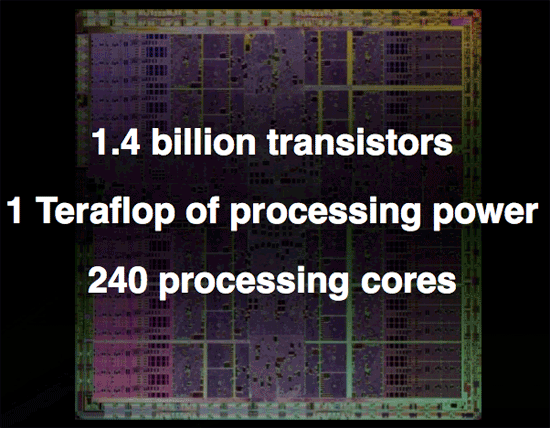
One-Point-Four-Billion. That's transistors folks.
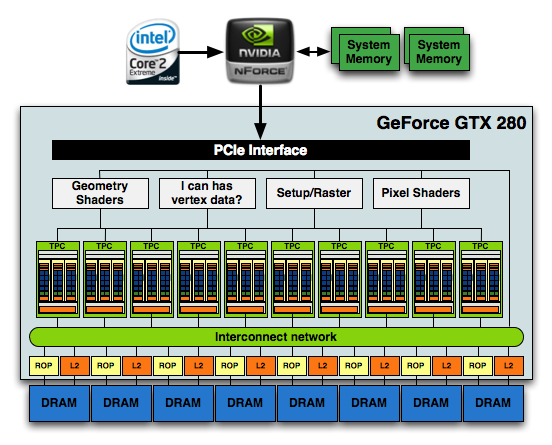
The chip is codenamed GT200 and it's the successor to NVIDIA's G80 and G92 families. Why the change in naming? The GT stands for "Graphics Tesla" and this is the second generation Graphics Tesla architecture, the first being the G80. The GT200 is launching today in two flavors, the die of the larger one is pictured below:
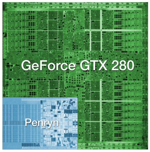
Um...yeah...we're reviewing that today
(this die comparison is to scale and that's a dual-core Penryn)
Let's put aside all the important considerations for a moment and bask in the glow of sheer geekdom. Intel's Montecito processor (their dual core Itanium 2) weighs in at over 1.7 billion transistors, but the vast majority of this is L3 cache (over 1.5 billion transistors for 24MB of on die memory). In contrast, the vast majority of the transistors on NVIDIA's GT200 chip are used for compute power. Whether or not NVIDIA has used these transistors well is certainly the most important consideration for consumers, but there's no reason we can't take a second to be in awe of the sheer magnitude of the hardware. This chip is packed full of logic and it is huge.
At most, 94 NVIDIA GT200 die can be produced on a single 300mm 65nm wafer from TSMC. On the other end of the spectrum, Intel can fit around 2500 45nm Atom processors on a 300mm wafer.
If the number of transistors wasn't enough to turn this thing into a dinner plate sized bit of hardware, the fact that it's fabbed on a 65nm process definitely puts it over the top. Current CPUs are at 45nm and NVIDIA's major competitor in the GPU market, AMD, has been building 55nm graphics chips for over 7 months now. With so many transistors, choosing not to shrink their manufacturing process doesn't seem to make much sense to us. Smaller fab processes offer not only the potential for faster, cooler chips, but also significantly reduce the cost of the GPU itself. Because manufacturing costs are (after ramping production) on a per wafer basis, the more dies that can be packed onto a single waffer, the less each die costs. It is likely that NVIDIA didn't want to risk any possible delays arising from manufacturing process changes on this cycle, but that seems like a risk that would have been worth taking in this case.
Instead, GT200 is the largest die TSMC has ever fabbed for production. Quite a dubious honor, and I wouldn't expect NVIDIA to really see this as something of which to be proud. Of course, that doesn't mean we can't be impressed with the sheer massiveness of the beast.
And what do we get from all these transistors? Moving up from 690M transistors of the original G80 and 754M transistors in G92 to the 1.4B transistors of GT200 is not a small tweak. One of the major new features is the ability to processes double precision floating point data in hardware (there are 30 64-bit FP units in GT200). The size of the register file for each SP array has been doubled. The promised ability of an SP to process a MAD and a MUL at the same time has been enhanced to work in more cases (G80 was supposedly able to do this, but the number of cases where it worked as advertised were extremely limited). And the number of SPs has increased from 128 on G80 to 240 with GT200. To better understand what all this means, we'll take a closer look at the differences between G80 and GT200, but first, the cards.
Clock Speeds, Pricing and HDMI Information
NVIDIA is introducing two GT200 parts today along with slightly tweaked branding. The new brand is called the GeForce GTX, and the first two cards are the GTX 280 and GTX 260.


Here's the card, say hello:
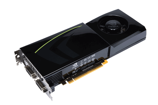
The GeForce GTX 280
It's got a little sibling too:

The GeForce GTX 260
The GeForce GTX 280 features 240 streaming processors running at 1.3GHz. It's got a 512-bit memory interface to 1GB of GDDR3 running at 2.2GHz (1107MHz core clock). The rest of the GPU runs at 602MHz.
| |
GTX 280 | GTX 260 | 9800 GX2 | 9800 GTX | 8800 GTS 512 | 8800 GT |
| Stream Processors | 240 | 192 | 256 | 128 | 128 | 112 |
| Texture Address / Filtering | 80 / 80 | 64 / 64 | 128 / 128 | 64 / 64 | 56 / 56 | 56 / 56 |
| ROPs | 32 | 28 | 32 | 16 | 16 | 16 |
| Core Clock | 602MHz | 576MHz | 600MHz | 675MHz | 650MHz | 600MHz |
| Shader Clock | 1296MHz | 1242MHz | 1500MHz | 1690MHz | 1625MHz | 1500MHz |
| Memory Clock | 1107MHz | 999MHz | 1000MHz | 1100MHz | 970MHz | 900MHz |
| Memory Bus Width | 512-bit | 448-bit | 256-bit x 2 | 256-bit | 256-bit | 256-bit |
| Frame Buffer | 1GB | 896MB | 1GB | 512MB | 512MB | 512MB |
| Transistor Count | 1.4B | 1.4B | 1.5B | 754M | 754M | 754M |
| Manufacturing Process | TSMC 65nm | TSMC 65nm | TSMC 65nm | TSMC 65nm | TSMC 65nm | TSMC 65nm |
| Price Point | $650 | $400 | $500 | $300 | $280 | $170-$230 |
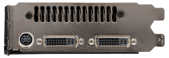
You'll need a power supply that can deliver up to 236W for the card itself and you'll need both a 6-pin and an 8-pin PCIe power connector (the board won't work with two 6-pin connectors).
The GeForce GTX 280 will retail for $650 with availability planned for June 17th.
The GTX 260 brings the total core count down to 192 by disabling two Texture/Processing Clusters on the GPU (but still maintaining more cores than any single-GPU G80/G92 based card). The SPs run slightly slower on the GTX 260 (1242MHz vs. 1296MHz, NVIDIA uses a 27MHz crystal so that's why we get these funny clock frequencies), while the memory runs at approximately 2GHz (999MHz memory clock, 1998MHz data rate). The GTX 260 also loses one of the 8 64-bit memory controllers, bringing the total memory bus down to 448-bits and total memory size down to 896MB.
The GTX 260 consumes a maximum of 183W and only needs two 6-pin power connectors. The GeForce GTX 260 will set you back $400 and should be available on June 26th.
The GTX 280's shroud, though it takes some cues from the 9800 GX2, is better engineered to allow for heat expulsion through a larger vent next to the IO ports. The 9800 GX2 didn't have a very wide opening to the outside world from which to remove heat. This resulted in the 9800 GX2 disproportionately increasing the heat of the system. Since we run our systems without cases we don't see problems like this as soon as our readers do, and we would like to thank you for pointing this out to us.
Both the GTX 260 and 280 have two dual-link DVI outputs, which can be converted to HDMI using an adapter if you'd like. You can pass SPDIF using a connector at the top of the card, which will then be passed to the HDMI output when using the DVI-HDMI adapter. For the HTPC enthusiasts out there, the GTX 280 and 260 can output the following audio formats over HDMI:
2-channel LPCM
6-channel DD bitstream
6-channel DTS bitstream
Unfortunately there's no support for 8-channel LPCM or bitstreaming of Dolby TrueHD or DTS HD-MA.
Building NVIDIA's GT200
Here's a Streaming Processor, NVIDIA calls it an SP:
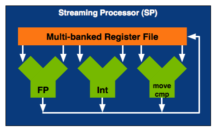
NVIDIA calls an individual SP a single processing core, which is actually true. It is a fully pipelined, single-issue, in-order microprocessor complete with two ALUs and a FPU. An SP doesn't have any cache, so it's not particularly great at anything other than cranking through tons of mathematical operations. Since an SP spends most of its time working on pixel or vertex data, the fact that it doesn't have a cache doesn't really matter. Aside from name similarities, one NVIDIA SP is a lot like a very simplified version of a SPE in the Cell microprocessor (or maybe the SPE is like a really simple version of one of NVIDIA's SMs, which we'll get to in a minute). While a single SPE in Cell has seven execution units, a single NVIDIA SP only has three.
By itself a SP is fairly useless, but NVIDIA builds GPUs and if you add up enough of these little monsters you can start to get something productive given that graphics rendering is a highly parallelizable task.
Here's a Streaming Multiprocessor, which NVIDIA abbreviates as SM:

A SM is an array of SPs, eight to be specific, along with two more processors called Special Function Units (SFUs). Each SFU has four FP multiply units which are used for transcendental operations (e.g. sin, cosin) and interpolation, the latter being used in some of the calculations for things like anisotropic texture filtering. Although NVIDIA isn't specific in saying so, we assume that each SFU is also a fully pipelined, single-issue, in-order microprocessor. There's a MT issue unit that dispatches instructions to all of the SPs and SFUs in the group.
In addition to the processor cores in a SM, there's a very small instruction cache, a read only data cache and a 16KB read/write shared memory. These cache sizes are kept purposefully small because unlike a conventional desktop microprocessor, the datasets we're trying to cache here are small. Each SP ends up working on an individual pixel and despite the move to 32-bit floating point values, there's only so much data associated with a single pixel. The 16KB memory is akin to Cell's local stores in that it's not a cache, but a software-managed data store so that latency is always predictable. With this many cores in a single SM, control and predictability and very important to making the whole thing work efficiently.
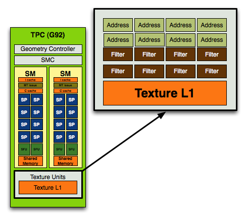
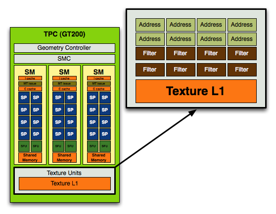
Take one more step back and you've got a Texture/Processor Cluster (TPC):
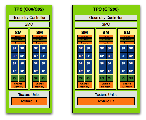
The G80/G92 TPC (left) vs. the GT200 TPC (right)
NVIDIA purposefully designed its GPU architecture to be modular, so a single TPC can be made up of any number of SMs. In the G80 architecture it was made up of two SMs but with the GT200 architecture it now has three SMs.
The components of the TPC however haven't changed; a TPC is made up of SMs, some control logic and a texture block. Remember that a SM is a total of 8 SPs and 2 SFUs, so that brings the total up to 24 SPs and 6 SFUs (must...not...type...STFU) per cluster in GT200 (up from 16 SPs and 4 SFUs in G80). The texture block includes texture addressing and filtering logic as well as a L1 texture cache.
The modular theme continues with the Streaming Processor Array (SPA) that is composed of a number of TPCs:
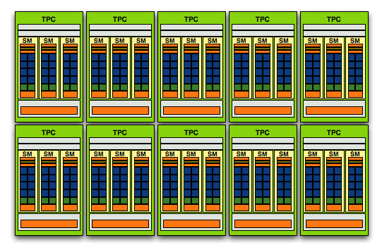
The GT200 SPA, that's 240 SPs in there if you want to count them
In G80 the SPA was made up of 8 TPCs, but with GT200 we've moved up to 10. Note that each TPC now has 3 SMs vs. 2, so the overall processing power of GT200 has increased by 87.5% over G80.
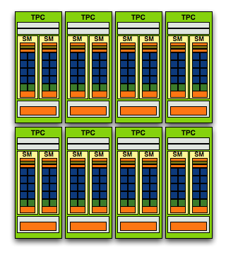
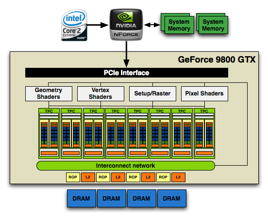
And here's G80/G92, only 128 SPs thanks to two SMs per TPC and 8 TPCs
At the front end of the GPU we've got schedulers and control logic to distribute workloads to the entire array of processing cores. At the other end we've got L2 texture caches and rasterization processors that handle final filtering and output of data to the frame buffer.
The culmination of all of this is that the new GT200 GPU, the heart of the GeForce GTX 280 and 260, features 240 SPs, 160KB of local memory, an even smaller amount of cache and is built on TSMC's 65nm process using 1.4 billion transistors.
1.4 Billion Transistors. It wants vertex data. Really bad.
754 Million Transistors
There are more transistors in this chip than there are people in China, and it's the largest, most compute-dense chip we've ever reviewed.
Lots More Compute, a Leetle More Texturing
NVIDIA's GT200 GPU has a significant increase in computational power thanks to its 240 streaming processors, up from 128 in the previous G80 design. As a result, NVIDIA's GT200 GPU showcases a tremendous increase in transistor count over its previous generation architecture (1.4 billion up from 686 million in G80).
The increase in compute power of GT200 is not mirrored however in the increase in texture processing power. On the previous page we outlined how the Texture/Processing Clusters went from two Shader Multiprocessors to three, and how there are now a total of ten TPCs in the chip up from 8 in the GeForce 8800 GTX.
In the original G80 core, used in the GeForce 8800 GTX NVIDIA's texture block looked like this:
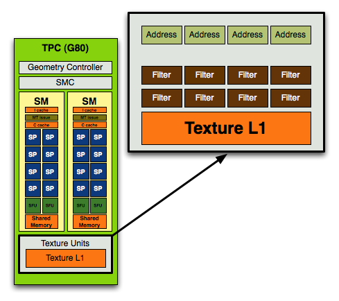
In each block you had 4 texture address units and 8 texture filtering units.
With the move to G92, used in the GeForce 8800 GT, 8800 GTS 512 and 9800 GTX, NVIDIA doubled the number of texture address units and achieved a 1:1 ratio of address/filtering units:
With GT200 in the GeForce GTX 280/260, NVIDIA kept the address-to-filtering ratio at 1:1 but increased the ratio of SPs to texture processors:
In the previous designs you'd have 8 address and 8 filtering units per TPC (or 16 streaming processors), in the GT200 you have the same 8 address and 8 filtering units but for a larger TPC with 24 SPs.
Here's how the specs stand up across the generations:
| NVIDIA Architecture Comparison | G80 | G92 | GT200 |
| Streaming Processors per TPC | 16 | 16 | 24 |
| Texture Address Units per TPC | 4 | 8 | 8 |
| Texture Filtering Units per TPC | 8 | 8 | 8 |
| Total SPs | 128 | 128 | 240 |
| Total Texture Address Units | 32 | 64 | 80 |
| Total Texture Filtering Units | 64 | 64 | 80 |
For a 87.5% increase in compute, there's a mere 25% increase in texture processing power. This ratio echoes what NVIDIA has been preaching for years: that games are running more complex shaders and are not as bound by texture processing as they were in years prior. If this wasn't true then we'd see a closer to 25% increase in performance of GT200 over G80 at the same clock rather than something much greater.
It also means that GT200's performance advantage over G80 or G92 based architectures (e.g. GeForce 9800 GTX) will be determined much by how computationally bound the games we're testing are.
The ratio of increase compute/texture power in the GT200 has been evident in NVIDIA architectures for years now, dating back to the ill-fated GeForce FX. NVIDIA sacrificed memory bandwidth on the GeForce FX, equipping it with a narrow 128-bit memory bus (compared to ATI's 256-bit interface on the Radeon 9700 Pro) and instead focused on building a much more powerful compute engine. Unfortunately, the bet was the wrong one to make at the time and the GeForce FX was hardly competitive (for more reasons than just a lack of memory bandwidth), but today we're dealing in a very different world. Complex shader programs run on each pixel on the screen and there's a definite need for more compute power in today's GPUs.
An Increase in Rasterization Throughput
In addition to the 25% increase in texture processing capabilities of the GT200, NVIDIA added two more ROP partitions to the GPU. While the GeForce 8800 GTX had six ROP partitions, each capable of outputting a maximum of 4 pixels per clock, the GT200 adds two more partitions.
With eight ROP partitions the GT200 can now output a maximum of 32 pixels per clock, up from 24 pixels per clock in the GeForce 8800 GTX and 9800 GTX.
The pixel blend rate on G80/G92 was half-speed, meaning that while you could output 24 pixels per clock, you could only blend 12 pixels per clock. Thanks to the 65nm shrink and redesign, GT200 can now output and blend pixels at full speed - that's 32 pixels per clock for each.
The end result is a non-linear performance improvement in everything from anti-aliasing and fire effects to shadows on GT200. It's an evolutionary change, but that really does sum up many of the enhancements of GT200 over G80/G92.
Derek Gets Technical: 15th Century Loom Technology Makes a Comeback
Because it's multithreaded...
Yes I know it's horrible, but NVIDIA has gone a bit deeper in explaining their architecture to us and they thought borrowing terminology from weaving was clever. But as much as that might make you want to roll your eyes, the explanation of how things work that is enabled is worth it.
In cloth weaving, a warp is the vertical group of parallel threads that are held taught while the weft are the threads passed through these. I suppose it makes sense, then, that NVIDIA decided to call their grouping of parallel threads to be executed on an SM a warp.
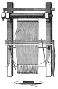
See the group of threads that hang from the top of this loom? That's called a warp.
With each SM having 8 SPs and G80 having two SMs per TPC (for a total of 16 SPs) it looked like a natural fit to execute quads across these 16 scalar units. We learned that this was not the case, but seeing the grouping of three SMs per TPC in GT200 still looked a little funny until we really learned more about how things are scheduled on NVIDIA's unified architecture. Each SM's scheduler picks a new warp to work on every clock cycle, and since the scheduler runs at half speed this ends up being every other clock cycle from the perspective of the rest of the SM. Each warp is made up of a group of 32 threads (in pixel shaders this is a group of 8 quads) that share an instruction stream (a shader program or a kernel if you're talking about GPU computing).
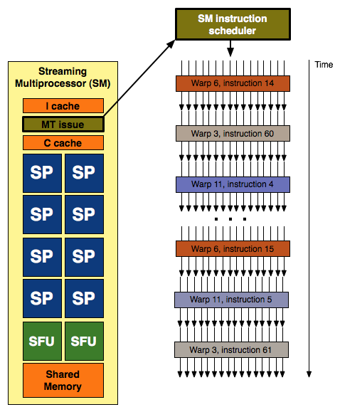
32 threads in a warp, issued in two groups of 16 threads - one such group is depicted above
Different warps built from threads executing the same shader program can follow completely independant paths down the code, but every thread within a warp must be exectuing the same instruction. This means that our branch granularity is 32 threads: every block of 32 threads (every warp) can branch independantly of all others, but if one or more threads within a warp branch in a different direction than the rest then every single thread in that warp must execute both code paths. Each threads only retains the result from the path it was supposed to follow probably by using the branch result to dynamically predicate the apporpriate path per thread. Each SM can have 32 (up from 24 in G80) warps in flight at the same time (for a total of 1024 threads in flight per SM). With 10 TPCs each containing 3 SMs, that's up to 30720 threads in flight on a GTX 280.
Each SM with it's 8 SPs and 2 SFUs is capable of processing up to 8 ops per clock (MAD (a fused floating point multiply and add) being the most complex) in the SPs and 8 ops per clock on the SFUs (which are made up of 4 floating point MUL units and other logic). Warps are executed on SMs in 2 groups of 16 threads (probably four quads for pixels) over four clock cycles.
This is where it gets interesting.
The SPs and SFUs are scheduled on alternating clock cycles from the perspective of the SM scheduler. They execute independent warps. SPs are scheduled on one clock cycle and SFUs are scheduled the next. Each is able to complete the processing of an entire warp before the next time it is scheduled, which happens to be four clocks (relative to the SPs and SFUs) after they it was scheduled with the last warp.
But wait ... aren't SMs supposed to be able to support dual-issue MAD+MUL? Well, back when G80 launched, Beyond3d did an excellent job of exploring the reality of the situation. With the fact that the SFU handles the "dual-issued" MUL and shares its time with other responsibilities like transcendental calculation and attribute interpolation, the ability of the hardware to actually accelerate cases that could take advantage of dual-issue was significantly reduced. But this scheduling revelation makes it clear that the problem is much more complex.
In order for code that could benefit from dual-issue hardware to take advantage of G80 or GT200, a warp must be scheduled on an SP for the MAD and then it must be re-scheduled on the SFU before it hits the SPs again. If the SFU is too busy handling attribute interpolation or transcendental math, then our warp will be rescheduled on the SPs to calculate the MUL and we will have lost our potential dual-issue speed up.
NVIDIA tells us that they "had some scheduling/issue problems with getting the MUL in the SFU to work consistently per clock. We fixed that in GT200." This makes perfect sense in light of what we now know about scheduling on G80/GT200. What they needed to do to improve the ability of their hardware to speed up cases where a MAD+MUL dual issue would help was to make sure that these cases were properly prioritized to execute on the SFU. We don't see MAD+MUL in every line of code, so giving these cases higher priority on the SFU than its other duties should help to optimize the utilization of the hardware. They do have to be careful not to start just running random MULs on the SFU because those special functions do still need to get done, but pushing a select subset of MULs onto the SFU (where they directly follow MADs that have just been executed on SPs) should definitely help in certain cases.
Really the main focus for NVIDIA is proper utilization and prioritization. Everything for any given frame needs to get done at some point or other, so simulating "dual-issue" shouldn't take priority over other things that need to get done that might be more important to completing the next frame. But organizing how to handle it is a big deal. Real time compilers are a big part of that, but internal thread management and scheduling in an architechure this wide also cannot be ignored. NVIDIA says they can now get 93-94% efficiency from their "dual-issue" implementation in directed tests and that this is significantly higher than on G80. Real world results will be lower, but the thing to remember is that the goal is simply to make maximally efficient use of the hardware availalbe. Just because the SFU isn't assisting in a MAD+MUL every clock doesn't mean it isn't doing something important.
This whole situation leaves us with mixed feelings. The hardware itself is not capable of "dual-issue" as it is understood in an architectural sense. The obfuscation of graphics hardware technology in a competitive industry has been the norm for the past decade, and we can accept this. We would prefer to know what the hardware is actually doing, but we are more than happy to have an explanation of something as a hardware feature where the hardware merely simulates the effect a specific architectural design has. But in the case where the hardware doesn't perform in nearly the same way as it would if the feature had actually been implemented as a hardware feature, we just can't help but be a little disappointed.
And we are conflicted about this because NVIDIA's design is actually very elegant. Attribute interpolation will always need to be done, and having hardware set aside for complex math is also very useful. But rather than making a dedicated fixed function interpolator or doing taylor expansion of complex math on SPs, NVIDIA built hardware that could serve both purposes and that had time left over to help offload some well placed MULs within the instruction stream of running programs.
If NVIDIA had been as open about their architecture as Intel is about their CPU designs, we could not have helped but to be impressed by this. The "missing MUL" wouldn't have been seen as a problem with NVIDIA's dual-issue "hardware"; we would have been praising NVIDIA's ability to schedule and multitask the different units within their SMs in order to improve utilization.
Tweaks and Enahancements in GT200
NVIDIA provided us with a list, other than the obvious addition of units and major enhancements in features and technology, of adjustments made from G80 to GT200. These less obvious changes are part of what makes this second generation Tesla architecture a well evolved G80. First up, here's a quick look at percent increases from G80 to GT200.
| NVIDIA Architecture Comparison | 8800 GTX | GTX 280 | % Increase |
| Cores | 128 | 240 | 87.5% |
| Texture | 64t/clk | 80t/clk | 25% |
| ROP Blend | 12p / clk | 32p / clk | 167% |
| Max Precision | fp32 | fp64 | |
| GFLOPs | 518 | 933 | 80% |
| FB Bandwidth | 86 GB/s | 142 GB/s | 65% |
| Texture Fill Rate | 37 GT/s | 48 GT/s | 29.7% |
| ROP Blend Rate | 7 GBL/s | 19 GBLs | 171% |
| PCI Express Bandwidth | 6.4 GB/s | 12.8GB/s | 100% |
| Video Decode | VP1 | VP2 |
Communication between the driver and the front-end hardware has been enhanced through changes to the communications protocol. These changes were designed to help facilitate more efficient data movement between the driver and the hardware. On G80/G92, the front-end could end up in contention with the "data assembler" (input assembler) when performing indexed primitive fetches and forced the hardware to run at less than full speed. This has been fixed with GT200 through some optimizations to the memory crossbar between the assembler and the frame buffer.
The post-transform cache size has been increased. This cache is used to hold transformed vertex and geometry data that is ready for the viewport clip/cull stage, and increasing the size of it has resulted in faster communication and fewer pipeline stalls. Apparently setup rates are similar to G80 at up to one primative per clock, but feeding the setup engine is more efficient with a larger cache.
Z-Cull performance has been improved, while Early-Z rejection rates have increased due to the addition of more ROPs. Per ROP, GT200 can eliminate 32 pixles (or up to 256 samples with 8xAA) per clock.
The most vague improvement we have on the list is this one: "significant micro-architectural improvements in register allocation, instruction scheduling, and instruction issue." These are apparently the improvements that have enabled better "dual-issue" on GT200, but that's still rather vague as to what is actually different. It is mentioned that scheduling between the texture units and SMs within a TPC has also been improved. Again, more detail would be appreciated, but it is at least worth noting that some work went into that area.
Register Files? Double Em!
Each of those itty-bitty SPs is a single-core microprocessor, and as such it has its own register file. As you may remember from our CPU architecture articles, registers are storage areas used to directly feed execution units in a CPU core. A processor's register file is its collection of registers and although we don't know the exact number that were in G80's SPs, we do know that the number has been doubled for GT200.
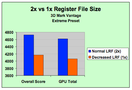
NVIDIA's own data shows a greater than 10% increase in performance due to the larger register file size (source: NVIDIA)
If NVIDIA is betting that games are going to continue to get more compute intensive, then register file usage should increase as well. More computations means more registers in use, which in turn means that there's a greater likelihood of running out of registers. If a processor runs out of registers, it needs to start swapping data out to much slower memory and performance suffers tremendously.
If you haven't gotten the impression that NVIDIA's GT200 is a compute workhorse, doubling the size of the register file per SP (multiply that by 240 SPs in the chip) should help drive the idea home.
Double the Precision, 1/8th the Performance
Another major feature of the GT200 GPU and cards based on it is support for hardware double precision floating point operations. Double precision FP operations are 64-bits wide vs. 32-bit for single precision FP operations.
Now the 240 SPs in GT200 are single-precision only, they simply can't accept 64-bit operations at all. In order to add hardware level double precision NVIDIA actually includes one double precision unit per shading multiprocessor, for a total of 30 double precision units across the entire chip.
The ratio of double precision to single precision hardware in GT200 is ridiculously low, to the point that it's mostly useless for graphics rasterization. It is however, useful for scientific computing and other GPGPU applications.
It's unlikely that 3D games will make use of double precision FP extensively, especially given that 8-bit integer and 16-bit floating point are still used in many shader programs today. If anything, we'll see the use of DP FP operations in geometry and vertex operations first, before we ever need that sort of precision for color - much like how the transition to single precision FP started first in vertex shaders before eventually gaining support throughout the 3D pipeline.
Geometry Wars
ATI's R600 is alright at geometry shading. So is RV670. G80 didn't really keep up in this area. Of course, games haven't really made extensive use of geometry shaders because neither AMD nor NVIDIA offered compelling performance and other techniques made more efficient use of the hardware. This has worked out well for NVIDIA so far, but they couldn't ignore the issue forever.
GT200 has enhanced geometry shading support over G80 and is now on par with what we wish we had seen last year. We can't fault NVIDIA too much as with such divergent new features they had to try and predict the usage models that developers might be interested in years in advance. Now that we are here and can see what developers want to do with geometry shading, it makes sense to enhance the hardware in ways that support these efforts.
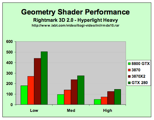
GT200 has significantly improved geometry shader performance compared to G80 (source: NVIDIA)
Generation of vertex data is a particularly weak part of NVIDIA's G80, so GT200 is capable of streaming out 6x the data of G80. Of course there are the scheduling enhancements that affect everything, but it is unclear as to whether NVIDIA did anything beyond increasing the size of their internal output buffers by 6x in order to enhance their geometry shading capability. Certainly this was lacking previously, but hopefully this will make heavy use of the geometry shader something developers are both interested in and can take advantage of.
Derek's Conjecture Regarding SP Pipelining and TMT
Temporal Multithreading
We know that the execution of instructions in each SP is pipelined. We know that the throughput of SPs is one instruction per clock cycle and that rather than stalling the pipeline the Tesla architecture usually doesn't need to wait for computational results or memory operations because it is highly likely another thread will be ready to execute. Context switches happen every four clocks from the perspective of the SPs within an SM, and in these four clocks each of the 32 threads in the currently active and executing warp will be serviced.
Organization of the executing threads isn't something we know except SMs process warps in two groups of 16 threads. That this point was made is of interest, but there are too many possibilites for us to come up with any real guess as to how they are issuing instructions to 8 physical SPs in groups of 16. Off hand we asked them if the SPs supported hardware level SMT (simultaneous multithreading) like hyperthreading and our answer was no but with a curious twist: "... they are pipelined processors and support many threads in progress in the pipeline." This was the light switch that brought together the realization of many potential advantages of this architecture for us.
If throughput is really one instruction per clock per SP, and each SP handles 4 threads from a warp over 4 clock cycles, then the pipeline is actually working on executing one instruction from a different thread at every stage in the pipeline.
This is actually a multithreading technique known as fine-grained TMT or temporal multithreading and is different than SMT in that it doesn't expose virtual parallel processors to the software but processes multiple threads in different time slices. TMT isn't some hot new technology you missed when it hit the scene: TMT is what computers have made use of for decades to process the many threads running on a single CPU concurrently without starving them. On a desktop CPU we are very familiar with course-grained multithreading where a single thread is serviced for a while before a context switch happens and another thread starts running. This context switch will normally occur after a certain number of cycles or if a higher priority thread needs the processor or if the thread needs to wait on IO or memory for something.
The real interesting bit comes in the differences between fine and course-grained TMT. In course-grained implementations (what we are all used to) all the pipeline stages of a processor are servicing an instruction stream from a single context, whereas in fine-grained we can have multiple context switches happening within the pipeline down to a context switch every stage. Making such fine-grained implementations happen can be tough, but NVIDIA has used a couple tricks to make it easier to manage.
In G80 and GT200, because of the fact that context is stored per warp, even though the SPs are working on an instruction for a different thread in every pipeline stage, they are not working on a different context at every pipeline stage. Each SP processes four threads in a row from the same warp and thus from the same context. Because it is incredibly likely at 1.5GHz that the SPs have more than 4 pipeline stages, we will still see more than one context switch within the pipeline itself, but it still isn't down to a different context for every stage.
So what's the big deal? Latency insensitivity and a maximal avoidance of pipeline bubbles and stalls.
In a modern CPU architecture, we see many instructions from the same thread running one after the other. If everything is running as smoothly as possible we have as many instructions retiring per clock cycle as we are capable of issueing per clock cycle, but this isn't gauranteed. Data dependancies, memory operations, cache misses and the like cause instructions to wait in the pipeline which means clock cycles go by without as much work as possible being done. Techniques to reduce this sort of delay are many. Data forwarding between pipeline stages is necessary to accomodate cases where one instruction is dependant on the result of the previous. This works by forwarding the result from one stage of the pipeline back to a previous stage so that instructions needing that data won't have to wait for it. Hyperthreading is even a technology to help increase pipeline utilization in that it makes one pipeline look like two different processors in order to fill it with more independent instructions and increase utilization.
Fine-grained TMT eliminates the need for data forwarding because there are zero dependant instructions coming down the pipeline: warps are context switched out after issuing one instruction for each independant thread and if NVIDIA's scheduler does its job right then warps won't be rescheduled until their data is available. Techniques like Hyperthreading are unnecessary because the pipeline is already full of instructions from independant threads at every stage.
Managing a pool of warps that are from a mix of different shader programs and different types of shaders (vertex, geometry and pixel) means that the chance every warp being serviced by an SM is wating on the same data is minimized, but having multiple warps from the same shader program is also a good idea to make sure that once data arrives it enables the processing of more than one warp. Of course, since SMs within one TPC share texture address, filter and cache, it is also a good idea to load up similar warps across the SMs on a TPC so that texture look ups by one thread might also be useful to many others. The balance here would be interesting to know, but we'll probably have to wait for Intel to enter the graphics market before we start getting confirmation on the really cool architectural aspects of all this.
How Deep is an SP?
As for pipeline depth, NVIDIA isn't helping us out with this one either, but let's walk through a little reasoning and see what we can come up with. At the insane and stupid extreme, we know NVIDIA wouldn't build a machine with a pipeline longer than they have threads in flight to fill. We'll assume G80 and GT200 are equally pipelined as they are clocked very similarly and we'll use what we know about G80 to draw a baseline. With G80 having 24 warps in flight per SM and each warp taking up 4 pipeline stages per SP, SPs can't possibly have more than 96 stages. Sure, that's crazy anyway, but if we expect that any warp executing in the pipeline won't be rescheduled until completion, then we would expect a higher proportion of warps to be waiting than executing.
If we go on this assumption we've got less than 48 stages, and I'd think it'd be fair to guess that they'd want to have at least two thrids of their their in-flight thread not in the pipeline, so that brings us down to a potential 32 stage pipeline. On the minimal end, there are at least 4 stages because if there were any less, high priority warps wouldn't get context switched at every opportunity: the instructions form the first threads scheduled would be completed and ready to go. Having 8 stages would give maximum flexibility as warps could be scheduled every other opportunity if they were otherwise ready. This would also keep at most three contexts active at different points in the pipeline, and while this type of fine-grained TMT does offer advantages, it is not free to implement a pipeline with access to a high number of contexts. And it is possible to design a single precision FP unit that can do a MAD in 8 cycles at 1.5GHz, but using Itanium as an example is usually seen as extravagant.
It would be tough to put a finer point on it without some indication from NVIDIA, but at least 8 and at most 32 stages is as good as we can get looking at their architecture. But knowing that power and performance per watt are key concerns of NVIDIA we can be fairly certain of eliminating anything higher than say 16 pipeline stages. Everyone remembers the space heater that was the Pentium 4 in general (and Prescott in particular), and it just isn't power efficient to go too deep.
By now we are at a fairly reasonable minimum of 8 stages and taking both architecture and power into consideration 16 seems like the max we could believe. Of course, that's all the way from one end of the world to the next. Anand's original guess was 12-15, but Derek was able to sell him on 8 stages as the sweet spot because of the simplicity of the cores (there are no decode or scheduling stages in the SPs). So was all that guessing about pipeline stages useful? Not really. But it sure was fun!
Now let's blow your mind and suggest that all this combined with the other details of NVIDIA's architecture suggest that all SP operations have the same latency. This way the entire thing would just work like a clock: one in, one out, very little overhead, and as simple as possible. All the overhead is managed outside the SP and the compute core can just focus on what it does best (as long as the rest of the chip does its job and keeps it fed).
UPDATE: We got lots of response on this page, and many CUDA developers, graphics software designers and hardware enthusiasts emailed us links to many resources on these topics. We discovered some very useful info: instruction latency is actually about 22 cycles in G80, so Anand and I were both way off. This and a couple other things we learned are available in our quick update on the GT200 pipeline published a couple days after this article first went live.
NVIDIA's Dirty Dealing with DX10.1 and How GT200 Doesn't Support it
I know many people were hoping to see DX10.1 implemented in GT200 hardware, but that is not the case. NVIDIA has opted to skip including some of the features of DX10.1 in this generation of their architecture. We are in a situation as with DX9 where SM2.0 hardware was able to do the same things as SM3.0 hardware albeit at reduced performance or efficiency. DX10.1 does not enable a new class of graphics quality or performance, but does enable more options to developers to simplify their code and it does enhance performance when coding certain effects and features.
It's useful to point out that, in spite of the fact that NVIDIA doesn't support DX10.1 and DX10 offers no caps bits, NVIDIA does enable developers to query their driver on support for a feature. This is how they can support multisample readback and any other DX10.1 feature that they chose to expose in this manner. Sure, part of the point of DX10 was to eliminate the need for developers to worry about varying capabilities, but that doesn't mean hardware vendors can't expose those features in other ways. Supporting DX10.1 is all or nothing, but enabling features beyond DX10 that happen to be part of DX10.1 is possible, and NVIDIA has done this for multisample readback and can do it for other things.
While we would love to see NVIDIA and AMD both adopt the same featureset, just as we wish AMD had picked up SM3.0 in R4xx hardware, we can understand the decision to exclude support for the features DX10.1 requires. NVIDIA is well within reason to decide that the ROI on implementing hardware for DX10.1 is not high enough to warrant it. That's all fine and good.
But then PR, marketing and developer relations get involved and what was a simple engineering decision gets turned into something ridiculous.
We know that both G80 and R600 both supported some of the DX10.1 featureset. Our goal at the least has been to determine which, if any, features were added to GT200. We would ideally like to know what DX10.1 specific features GT200 does and does not support, but we'll take what we can get. After asking our question, this is the response we got from NVIDIA Technical Marketing:
"We support Multisample readback, which is about the only dx10.1 feature (some) developers are interested in. If we say what we can't do, ATI will try to have developers do it, which can only harm pc gaming and frustrate gamers."
The policy decision that has lead us to run into this type of response at every turn is reprehensible. Aside from being blatantly untrue at any level, it leaves us to wonder why we find ourselves even having to respond to this sort of a statement. Let's start with why NVIDIA's official position holds no water and then we'll get on to the bit about what it could mean.
The statement multisample readback is the only thing some developers are interested in is untrue: cube map arrays come in quite handy for simplifying and accelerating multiple applications. Necessary? no, but useful? yes. Separate per-MRT blend modes could become useful as deferred shading continues to evolve, and part of what would be great about supporting these features is that they allow developers and researchers to experiment. I get that not many devs will get up in arms about int16 blends, but some DX10.1 features are interesting, and, more to the point, would be even more compelling if both AMD and NVIDIA supported them.
Next, the idea that developers in collusion with ATI would actively try to harm pc gaming and frustrate gamers is false (and wreaks of paranoia). Developers are interested in doing the fastest most efficient thing to get their desired result with as little trouble to themselves as possible. If a techique makes sense, they will either take it or leave it. The goal of a developer is to make the game as enjoyable as possible for as many gamers as possible, and enabling the same experience on both AMD and NVIDIA hardware is vital. Games won't come out with either one of the two major GPU vendors unable to run the game properly because it is bad for the game and bad for the developer.
Just like NVIDIA made an engineering decision about support for DX10.1 features, every game developer must weight the ROI of implementing a specific feature or using a certain technique. With NVIDIA not supporting DX10.1, doing anything DX10.1 becomes less attractive to a developer because they need to write a DX10 code path anyway. Unless a DX10.1 code path is trivial to implement, produces the same result as DX10, and provides some benefit on hardware supporting DX10.1 there is no way it will ever make it into games. Unless there is some sort of marketing deal in place with a publisher to unbalance things which is a fundamental problem with going beyond developer relations and tech support and designing marketing campaigns based on how many games dispaly a particular hardware vendors logo.
The idea that NVIDIA is going to somehow hide the capabilities of their hardware from AMD is also naive. The competition through the use of xrays, electron microscopes and other tools of reverse engineering are going to be the first to discover all the ins and outs of how a piece of silicon works once it hits the market. NIVIDA knows AMD will study GT200 because NVIDIA knows it would be foolish for them not to have an RV670 core on their own chopping block. AMD will know how best to program GT200 before developers do and independantly of any blanket list of features we happen to publish on launch day.
So who really suffers from NVIDIA's flawed policy of silence and deception? The first to feel it are the hardware enthusiasts who love learning about hardware. Next in line are the developers because they don't even know what features NVIDIA is capable of offering. Of course, there is AMD who won't be able to sell developers on support for features that could make their hardware perform better because NVIDIA hardware doesn't support it (even if it does). Finally there are the gamers who can and will never know what could have been if a developer had easy access to just one more tool.
So why would NVIDIA take this less than honorable path? The possibilities are endless, but we're happy to help with a few suggestions. It could just be as simple as preventing AMD from getting code into games that runs well on their hardware (as may have happened with Assassin's Creed). It could be that the features NVIDIA does support are incredibly subpar in performance: just because you can do something doesn't mean you can do it well and admitting support might make them look worse than denying it. It could be that the fundamental architecture is incapable of performing certain basic functions and that reengineering from the ground up would be required for DX10.1 support.
NVIDIA insists that if it reveals it's true feature set, AMD will buy off a bunch of developers with its vast hoards of cash to enable support for DX10.1 code NVIDIA can't run. Oh wait, I'm sorry, NVIDIA is worth twice as much as AMD who is billions in debt and struggling to keep up with its competitors on the CPU and GPU side. So we ask: who do you think is more likely to start buying off developers to the detriment of the industry?
GT200 vs. G80: A Clock for Clock Comparison
The GT200 architecture isn't tremendously different from G80 or G92, it just has a lot more processing power. The comparison below highlights the clock for clock difference between GT200 and its true predecessor, NVIDIA's G80. We clocked both GPUs at 575MHz core, 900MHz memory and 1350MHz shader, so this is a look at the hardware's architectural enhancements combined with the pipeline and bus width increases. The graph below shows the performance advantage of GT200 over G80 at the same clock speeds:
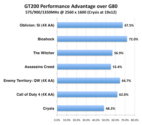
Clock for clock, just due to width increases, we should be at the very worst 25% faster with GT200. This would be the case where we are texture bound. It is unlikely an entire game will be blend rate bound to the point where we see greater than 2x speedups, and while test cases could show this real world apps just aren't blend bound. More realistically, the 87.5% increase in SPs will be the upper limit on performance improvements at the same clock rate. We see our tests behave within these predicted ranges.
Based on this, it appears that Bioshock is quite compute bound and doesn't run into many other bottlenecks when the burden is eased. Crysis on the other hand seems to be limited by more than just compute as it didn't benefit quite as much.
The way compute has been rebalanced does affect the conditions under which performance will benefit from the additional units. More performance will be available in the case where a game didn't just need more compute, but it needed more computer per texture. The converse is true when a game could benefit from more compute, but only if there was more texture hardware to feed them.
Power and Power Management
Power is a major concern of many tech companies going forward, and just adding features "because we can" isn't the modus operandi anymore. Now it's cool (pardon the pun) to focus on power management, performance per watt, and similar metrics. To that end, NVIDIA has beat their GT200 into such submission that it's 2D power consumption can reach as low as 25W. As we will show below, this can have a very positive impact on idle power for a very powerful bit of hardware.
These enhancements aren't breakthorugh technologies: NVIDIA is just using clock gating and dynamic voltage and clock speed adjustment to achieve these savings. There is hardware on the GPU to monitor utilization and automatically set the clock speeds to different performance modes (either off for hybrid power, 2D/idle, HD video, or 3D/performance). Mode changes can be done on the millisecond level. This is very similar to what AMD has already implemented.
With increasing transistor count and huge GPU sizes with lots of memory, power isn't something that can stay low all the time. Eventually the hardware will actually have to do something and then voltages will rise, clock speed will increase, and power will be converted into dissapated heat and frames per second. And it is hard to say what is more impressive, the power saving features at idle, or the power draw at load.
There is an in between stage for HD video playback that runs at about 32W, and it is good to see some attention payed to this issue specifically. This bodes well for mobile chips based off of the GT200 design, but in the desktop this isn't as mission critical. Yes reducing power (and thus what I have to pay my power company) is a good thing, but plugging a card like this into your computer is like driving an exotic car: if you want the experience you've got to pay for the gas.
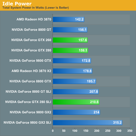
Idle power so low is definitely nice to see. Having high end cards idle near midrange solutions from previous generations is a step in the right direction.
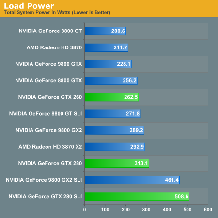
But as soon as we open up the throttle, that power miser is out the door and joules start flooding in by the bucket.
Cooling NVIDIA's hottest card isn't easy and you can definitely hear the beast moving air. At idle, the GPU is as quiet as any other high-end NVIDIA GPU. Under load, as the GTX 280 heats up the fan spins faster and moves much more air, which quickly becomes audible. It's not GeForce FX annoying, but it's not as quiet as other high-end NVIDIA GPUs; then again, there are 1.4 billion transistors switching in there. If you have a silent PC, the GTX 280 will definitely un-silence it and put out enough heat to make the rest of your fans work harder. If you're used to a GeForce 8800 GTX, GTS or GT, the noise will bother you. The problem is that returning to idle from gaming for a couple of hours results in a fan that doesn't want to spin down as low as when you first turned your machine on.
While it's impressive that NVIDIA built this chip on a 65nm process, it desperately needs to move to 55nm.
The Test
| Test Setup | |
| CPU | Intel Core 2 Extreme
QX9770 @ 3.20GHz |
| Motherboard | EVGA nForce 790i SLI |
| Video Cards | ATI Radeon HD 3870
X2 ATI Radeon HD 3870 NVIDIA GeForce 9800 GTX NVIDIA GeForce 9800 GX2 NVIDIA GeForce 8800 GTX NVIDIA GeForce 8800 GT NVIDIA GeForce GTX 280 NVIDIA GeForce GTX 260 |
| Video Drivers | Catalyst 8.5 ForceWare 177.34 (for GT200) ForceWare 175.16 (everything else) |
| Hard Drive | Seagate 7200.9 120GB 8MB 7200RPM |
| RAM | 4 x 1GB Corsair DDR3-1333 7-7-7-20 |
| Operating System | Windows Vista Ultimate
64-bit SP1 |
| PSU | OCZ EliteXStream 1000W (did not work with GTX 280 SLI) |
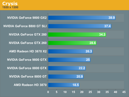
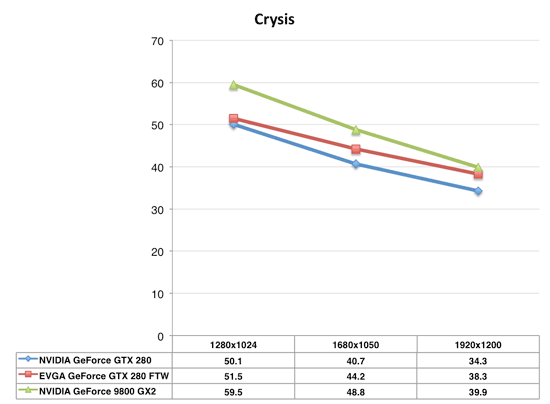
Crysis
Crysis is finally getting to be a little more playable here, but what shouldn't be too surprising is that the GeForce GTX 280 actually loses to the GeForce 9800 GX2 here. Remember that the GX2 has more processing power thanks to its dual GPUs and although it has less usable memory bandwidth, the overall performance here is more processing bound and thus the GX2 pulls ahead. Keep in mind that the GX2 is at least $150 cheaper than the GTX 280 and you'll quickly realize that as impressive of an architecture as the GT200 is, the price point just doesn't seem to be right.
The GeForce GTX 260 does very well in Crysis, slightly outperforming the Radeon HD 3870 X2. At $400, this is a much closer race and one that's a lot harder to call, so let's move on.
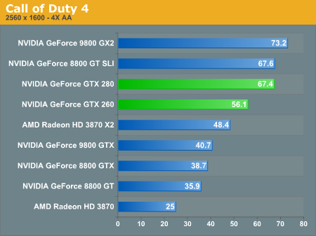
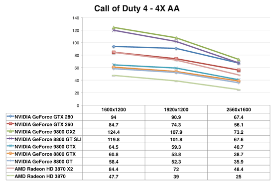
Call of Duty 4
We may be seeing the beginnings of a trend here, the GX2 continues to outperform the GTX 280, while the GTX 260 pulls ahead of the Radeon HD 3870 X2. If you've got an NVIDIA platform however, a pair of 8800 GTs are cheaper and will significantly outperform not only the GTX 260 but also the more expensive 280.
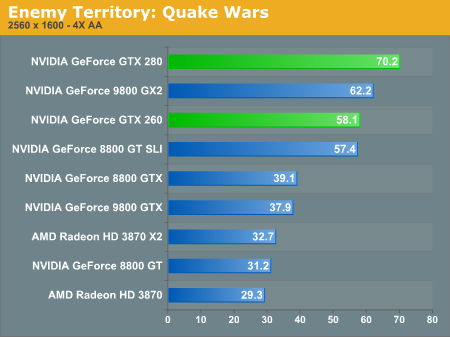
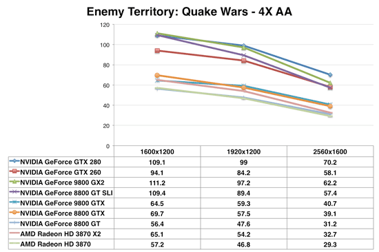
Enemy Territory: Quake Wars
We finally have a win for the GTX 280 over the GX2 and it's a healthy one at that. ET:QW appears to be more memory bandwidth bound and thus the GX2 falls behind. ATI continues to have problems under Quake Wars and the 3870 X2 stops being a threat to NVIDIA, the GTX 260 however ends up performing like a pair of GeForce 8800 GTs.
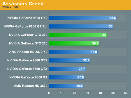
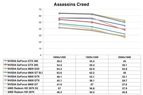
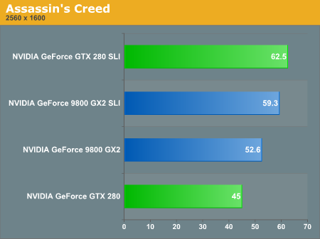
Assassin's Creed
With Assassin's Creed we're back to normal - the 9800 GX2 is on top, generally outperforming the GTX 280. Assassin's Creed scales well with multiple GPUs and thus even the 8800 GT SLI can outperform the GTX 280 here. A pair of 8800 GTs actually have more processing power than a single GTX 280, despite having fewer SPs. While the GTX 280 has 240 SPs to the 8800 GTs 112 (or 224 in SLI), the GTX 280 runs its SPs at just under 1.3GHz while the 8800 GT runs them at 1.5GHz.
The GTX 260 manages to outperform the Radeon HD 3870 X2, but obviously also loses to the 8800 GT SLI.
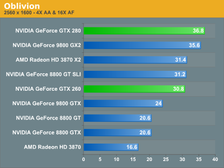
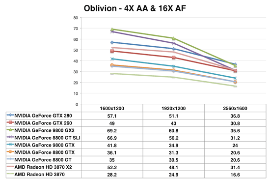
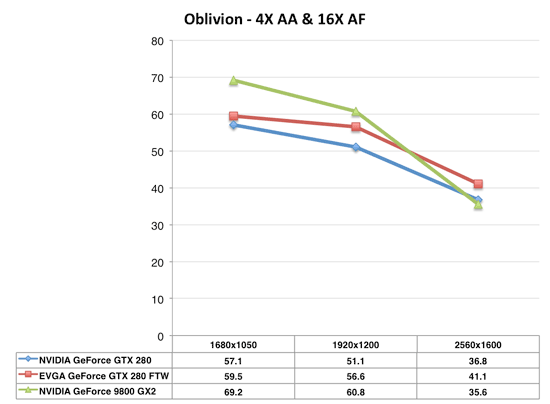
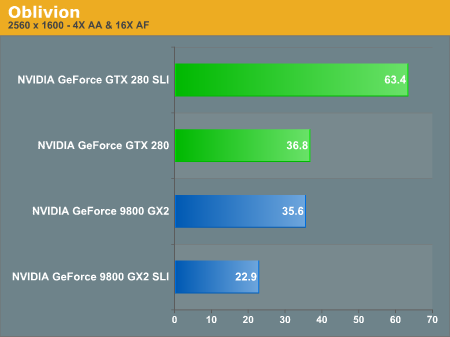
Oblivion
The race is pretty close between the GTX 280 and 9800 GX2 in Oblivion with AA enabled. It's worth noting that at all other resolutions, the GX2 is faster than the GTX 280 but at 2560 x 1600 the memory bandwidth requirements are simply too much for the GX2. Remember that despite having two GPUs, the GX2 doesn't have a real world doubling of memory bandwidth.
The GTX 260 performs like a Radeon HD 3870 X2 and 8800 GT SLI here. Once again it's one card performing like two, it's just that the two card solution is actually cheaper. Hmm...a great way to sell more SLI motherboards.
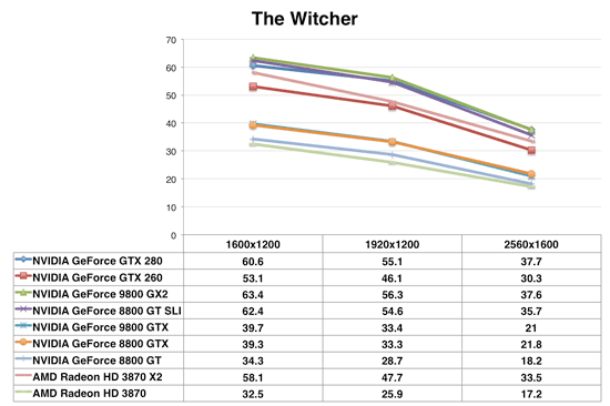
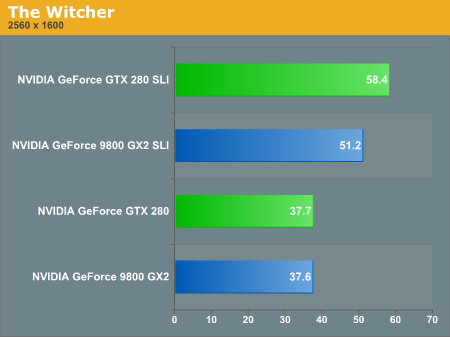
The Witcher
The GTX 280 continues to hang with the 9800 GX2, while the GTX 260 falls short of both the 8800 GT SLI or the 3870 X2 in The Witcher.

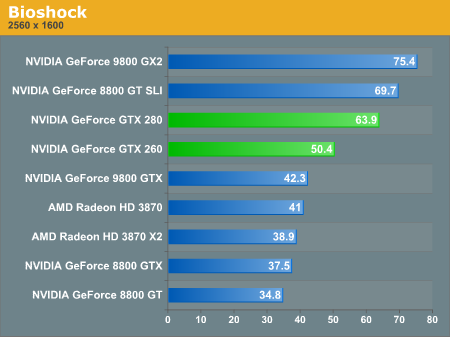
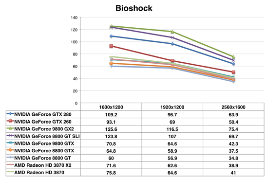
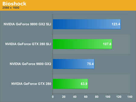
Bioshock
From a value standpoint, our final benchmark is particularly disappointing for the new GeForce GTX lineup. The 280 is still slower than the 9800 GX2 and actually even the 8800 GT SLI, and the 260 is considerably slower than that. Both are NVIDIA's fastest single-card, single-GPU solutions, but not the best value NVIDIA has to offer at the high end.
Overclocked: EVGA GeForce GTX 280 FTW
EVGA was kind enough to send us a card so that we could test SLI and take a look at overclocked performance of the GTX 280. Their card uses the stock HSF, but has fairly high clock speeds:
| Stock GTX 280 | EVGA GeForce GTX 280 FTW | % Increase | |
| GPU Clock | 602MHz | 670MHz | 11.3% |
| Shader Clock | 1296MHz | 1458MHz | 12.5% |
| Memory Clock | 1107MHz | 1215MHz | 9.8% |


We ran a few quick tests to look at overclocking performance and we saw about an 8% to 12% increase in a few games at high resolutions over the stock clocked card. Here is a quick look at a couple of these tests.
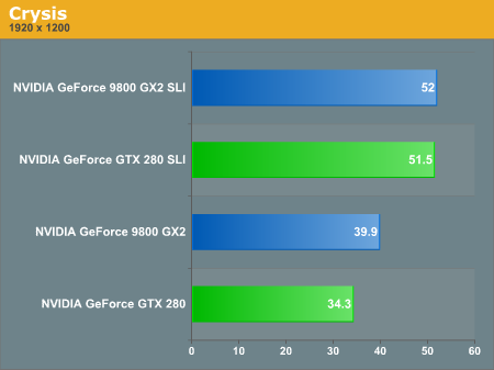
Crysis is one of many benchmarks where the GTX 280 falls behind the GeForce 9800 GX2, unfortunately even an overclocked GTX 280 will not dethrone the almighty GX2.
Oblivion on the other hand showcases a memory bandwidth limitation of the GX2 at ultra high resolutions, here we see an 11% performance advantage from the overclocked EVGA card. Given that the EVGA card has an average clock speed increase of 11.2%, this sort of a performance gain isn't bad at all. Even at 1920 x 1200 we see a 9% performance improvement from the overclocked card.
It seems as if the GTX 280 and GTX 260 can stand to benefit from overclocking very well.
SLI Performance Throwdown: GTX 280 SLI vs. 9800 GX2 Quad SLI
We had two GeForce GTX 280s on hand and a plethora of SLI bridges, so we of course had to run them in SLI. Now remember that a single GTX 280 uses more power than a GeForce 9800 GX2, and thus two of them is going to use a lot of power. It was so much power in fact that our OCZ EliteXStream 1000W power supply wasn't enough. While the SLI system would boot and get into Windows, we couldn't actually complete any benchmarks. All of the power supplies on the GTX 280 SLI certified list are at least 1200W units. We didn't have any on hand so we had to rig up a second system with a separate power supply and used the second PSU to power the extra GTX 280 card. A 3-way SLI setup using GTX 280s may end up requiring a power supply that can draw more power than most household circuits can provide.
Although a single GeForce GTX 280 loses to a GeForce 9800 GX2 in most cases, scaling from two to four GPUs is never as good as scaling from one to two. Thus forcing the question: are a pair of GTX 280s in SLI faster than a 9800 GX2 Quad SLI setup?
Let's look at the performance improvements from one to two cards across our games:
| GTX 280 SLI (Improvement from 1 to 2 cards) | 9800 GX2 SLI (Improvement from 1 to 2 cards) |
|
| Crysis | 50.1% | 30.3% |
| Call of Duty 4 | 62.8% | 64.0% |
| Assassin's Creed | 38.9% | 12.7% |
| The Witcher | 54.9% | 36.2% |
| Bioshock | 68.4% | 63.7% |
| Oblivion | 72.3% | -35.7% |
Crysis, Assassin's Creed, The Witcher and Oblivion are all situations where performance either doesn't scale as well or drops when going from one to two GX2s, giving NVIDIA a reason to offer two GTX 280s over a clumsy Quad SLI setup.
Thanks to poor Quad SLI scaling, the GX2 SLI and the GTX 280 SLI perform the same, despite the GTX 280 being noticeably slower than the 9800 GX2 in single-card mode.

When it does scale well however, the GX2 SLI outperforms the GTX 280 SLI setup just as you'd expect.
Sometimes you run into serious issues with triple and quad SLI where performance is actually reduced; Oblivion at 2560 x 1600 is one of those situations and the result is the GTX 280 SLI gives you a better overall experience.
While we'd have trouble recommending a single GTX 280 over a single 9800 GX2, a pair of GTX 280s will probably give you a more hassle-free, and consistent experience than a pair of 9800 GX2s.
Folding@home Now on NVIDIA
Folding@home, for those who don't know, is a distributed computing app designed to help researchers better understand the process of protien folding. Knowing more about how protiens assemble themselves can help us better understand many diseases such as alzheimers, but protien folding is very complex and takes a long time to simulate. the problem is made much easier by breaking it up into smaller parts and allowing many people to work on the problem.
Most of this work has been done on the CPU, but PS3 and AMD R5xx GPUs have been able to fold for a while now. Recently support for AMD's R6xx lineup was added as well. NVIDIA GPUs haven't been enabled to run folding@home until now (or very soon anyway). Stanford has finally implemented a version of folding@home with CUDA support that will allow all G80 and higher hardware to run the client.
We've had the chance for the past couple days to play around with a pre-beta version of the folding client, and running folding on NVIDIA hardwarwe is definitly very fast. Work units and protiens are different on CPUs and GPUs because the hardware is suited to different tasks, but to give some perspective a quadcore CPU could simulate tens of nanoseconds of a protien fold, while GPUs can simulate hundreds.
While we don't have the ability to bring you any useful comparative benchmarks right now, Stanford is working on implemeting some standard test cases that can be run on different hardware. This will help us actually compare the performance of different hardware in a meaningful way. Right now giving you numbers to compare CPUs, PS3s, AMD and NVIDIA GPUs would be like directly comparing framerates from different games on different hardware as if they were related.
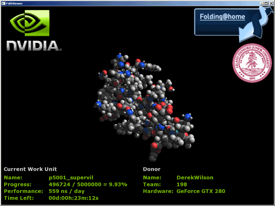
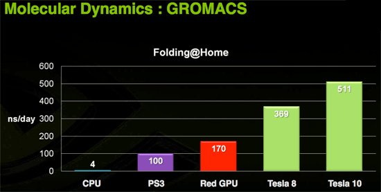
What we will say is that NVIDIA predicts that the GTX 280 will be capable of simulating something between 5 and 6 hundred nanoseconds of folding per day while CPUs are going to be two orders of magnitude slower. They also show the GTX 280 handily ahead of any current AMD solutions by high margins, but until we can test it ourselves we really don't want to put a finer point on it.
In our tests, we've actually seen the GT200 folding client perform at between 600 and 850ns per day (using the timestamps in the log file to determine performance), so we are quite impressed. Work units complete about every 20 to 25 minutes depending on the protien and whether or not the viewer is running (which does have a significant impact since the calculations and the display are both running on the GPU).
Hardware H.264 Encoding
For years now both ATI and NVIDIA have been boasting about how much better their GPUs were for video encoding than Intel's CPUs. They promised multi-fold speedups in performance but never delivered, so we've been stuck encoding and transcoding videos on CPUs.
With the GT200, NVIDIA has taken one step closer to actually delivering on these promises. We got a copy of a severely limited beta of Elemental Technologies' BadaBOOM Media Converter:
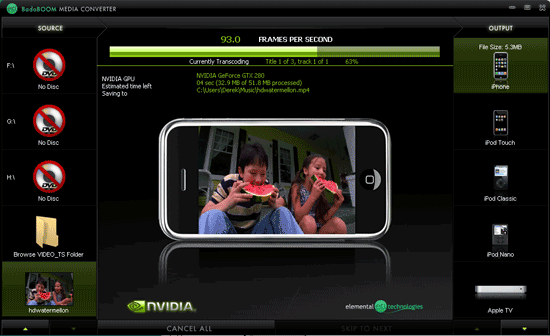
The media converter currently only works on the GeForce GTX 280 and GTX 260, but when it ships there will be support for G80/G92 based GPUs as well. The arguably more frustrating issue with it today is its lack of support for CPU-based encoding, so we can't actually make an apples-to-apples comparison to CPUs or other GPUs. The demo will also only encode up to 2 minutes of video.
With that out of the way however, BadaBOOM will perform H.264 encoding on your GPU. There is still a significant amount of work being done on the CPU during the encode, our Core 2 Extreme QX9770 was at 20 - 30% CPU utilization during the entire encode process, but it's better than the 50 - 100% it would normally be at if we were encoding on the CPU alone.
Then there's the speedup. We can't perform a true apples-to-apples comparison since we can't use BadaBOOM's H.264 encoder on anything else, but compared to using the open source x264 encoder the performance speedup is pretty good. We used AutoMKV and played with its presets to vary quality:
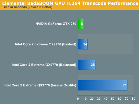
In the worst case scenario, the GTX 280 is around 40% faster than encoding on Intel's fastest CPU alone. In the best case scenario however, the GTX 280 can complete the encoding task in 1/10th the time.
We're not sure where a true apples-to-apples comparison would end up, but somewhere between those two extremes is probably a good guesstimate. Hopefully we'll see more examples of GPU based video encoder applications in the future as there seems to be a lot of potential here. Given how long it takes to encode a Blu-ray movie, we needn't even explain why it's necessary.
Overclocked and 4GB of GDDR3 per Card: Tesla 10P
Now let's say that you want to get some real work done with NVIDIA's GT200 GPU but that 1.4 billion transistor chip just isn't enough. NVIDIA does have an answer for you, in the form of an overclocked GT200 with the 240 SPs running at 1.5GHz (up from 1.3GHz in the GTX 280) and with a full 4GB of GDDR3 memory on-board.
Today NVIDIA is also announcing their next generation Tesla product based on GT200 (called a T10P when used on Tesla for some reason). The workstation graphics guys will have to wait a while for a GT200 Quadro unfortunately. This new Tesla is similar to the older model in that it has much more RAM and no IO ports. The server version is also clocked higher than the desktop part because fan noise isn't an issue and data centers have lower ambient temperatures than some corner of an office under a desk.
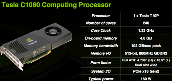
The Tesla C1060 has an entire 4GB of RAM on board. This is obviously very large and will do well to accomodate the large scale scientific computing apps it is targeted at. This card is designed for use in workstations and is the little brother to the new monster server that is also being announced today.
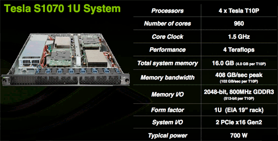
The Tesla S1070 is a 1U server containing essentially 4 C1060 cards for a total of 16GBs of RAM on 960 SPs. This server, like the older version, connects to a server via a PCIe cable and is designed to run code written for CUDA at incredible speeds. With 120 double precision IEEE 754r floating point units in combination with the 960 single precision IEEE 754 units, this server is a viable option for many more projects than the previous Tesla hardware which was only capable of single precision floating point.
Though we don't have an application to benchmark the double precision floating point hardware on GT200 yet, NVIDIA states that a GT200 can roughly match an 8 core Xeon system in DP performance. This would put the S1070 on par with a 32 way Xeon setup at less than 700W. Needless to say, single precision code runs much much faster and can outpace hundreds of traditional CPUs in parallel.
While these servers are expensive (though we don't have pricing), they are cheap compared to the alternatives currently out there. The fact that CUDA code can be implemented and tested on any of the 70 million NVIDIA G80+ GPUs currently in people's hands means that developer already have a platform to test and debug code on before committing to the Tesla solution. On top of that, schools are beginning to adopt CUDA as a teaching tool for parallel computing. As CUDA gains acceptance and the benefits of GPU computing are realized, more and more major markets will take interest.
The graphics card is no longer a toy. The combination of CUDA's academic acceptance as a teaching tool and the availability of 64-bit floating point in GT200 make GPUs a mission critical computing tool that will act as a truly disruptive technology. Not only will many major markets that depend on high performance floating-point processing realize this, but every consumer with an NVIDIA graphics card will be able to take advantage of hundreds of gigaflops of performance from CUDA based consumer applications.
Today we have folding@home and soon we'll have Elemental's transcoder. Imagine the audio and video processing capabilities of a PC if the GPU were actively used in software like ProTools and Premier. Open source programs could easily best the processing capabilities of many solutions with dedicated hardware for these types of applications.
Of course, the major limiter to the adoption of this technology is that it is vendor specific. If NVIDIA put the time in (or enlisted help) to make CUDA an ANSI or ISO standard extention to a programming language, we would could really start to get excited. Beyond that, the holy grail would be a unification of virtualized instruction sets creating a standard low level "assembly" interface for GPU computing allowing CUDA to compile to one target and run on any graphics card. Sort of an x86 for massively parallel work.
Right now CUDA compiles to PTX, NVIDIA's virtual instruction set, and there is no reason someone couldn't write a CUDA compiler to target AMD's equivalent CAL (or even to develop a PTX to CAL wrapper that allowed AMD GPUs to run compiled CUDA code). Unfortunately, NVIDIA doesn't want to invest money and resources in extending functionality to AMD and AMD doesn't want to invest money and resources into bolstering an NVIDIA owned technology (that could theoretically radically change to cripple AMD's hardware support in future versions). While standards and cooperation are a great idea, the competition in this market is such that neither NVIDIA nor AMD are looking to take a chance on benefiting the consumer if there is any risk of strenthening the competition (even in spite of weakening the industry).
Final Words
There's no question that NVIDIA has built a very impressive chip with the GT200. As the largest microprocessor we've ever reviewed, NVIDIA has packed an unreal amount of computational horsepower into the GT200. What's even more impressive is that we can fully expect NVIDIA to double transistor count once again in about 18 months, and once more we'll be in this position of complete awe of what can be done. We're a little over a decade away from being able to render and display images that would be nearly indistinguishable from reality, and it's going to take massive GPUs like the GT200 to get us there.
Interestingly, though, AMD has decided to make public its decision to go in the opposite direction. No more will ATI be pushing as many transistors as possible into giant packages in order to do battle with NVIDIA for the coveted "halo" product that inspires the masses to think an entire company is better because they made the fastest possible thing regardless of value. The new direction ATI will go in will be one that it kind of stumbled inadvertently into: providing midrange cards that offer as high a performance per dollar as possible.
With AMD dropping out of the high end single-GPU space (they will still compete with multiGPU solutions), NVIDIA will be left all alone with top performance for the forseable future. But as we saw from our benchmarks, that doesn't always work out quite like we would expect.
There's another very important aspect of GT200 that's worth considering: a die-shrunk, higher clocked version of GT200 will eventually compete with Intel's Larrabee GPU. The GT200 is big enough that it could easily smuggle a Penryn into your system without you noticing, which despite being hilarious also highlights a very important point: NVIDIA could easily toss a high performance general purpose sequential microprocessor on its GPUs if it wanted to. At the same time, if NVIDIA can build a 1.4 billion transistor chip that's nearly 6x the size of Penryn, so can Intel - the difference being that Intel already has the high performance, general purpose, sequential microprocessor that it could integrate alongside a highly parallel GPU workhorse. While Intel has remained relatively quiet on Larrabee as of late, NVIDIA's increased aggressiveness towards its Santa Clara neighbors is making more sense every day.
We already know that Larrabee will be built on Intel's 45nm process, but given the level of performance it will have to compete with, it wouldn't be too far fetched for Larrabee to be Intel's first 1 - 2 billion transistor microprocessor for use in a desktop machine (Nehalem is only 781M transistors).
Intel had better keep an eye on NVIDIA as the GT200 cements its leadership position in the GPU market. NVIDIA hand designed the logic that went into much of the GT200 and managed to produce it without investing in a single fab, that is a scary combination for Intel to go after. It's not to say that Intel couldn't out engineer NVIDIA here, but it's just going to be a challenging competition.
NVIDIA has entered a new realm with the GT200, producing a world class microprocessor that is powerful enough to appear on even Intel's radar. If NVIDIA had the ability to enable GPU acceleration in more applications, faster, then it would actually be able to give Intel a tough time before Larrabee. Fortunately for Intel, NVIDIA is still just getting started on moving into the compute space.
But then we have the question of whether or not you should buy one of these things. As impressive as the GT200 is, the GeForce GTX 280 is simply overpriced for the performance it delivers. It is NVIDIA's fastest single-card, single-GPU solution, but for $150 less than a GTX 280 you get a faster graphics card with NVIDIA's own GeForce 9800 GX2. The obvious downside to the GX2 over the GTX 280 is that it is a multi-GPU card and there are going to be some situations where it doesn't scale well, but overall it is a far better buy than the GTX 280.
Even looking to the comparison of four and two card SLI, the GTX 280 doesn't deliver $300 more in value today. NVIDIA's position is that in the future games will have higher compute and bandwidth requirements and that the GTX 280 will have more logevity. While that may or may not be true depending on what actually happens in the industry, we can't recommend something based on possible future performance. It just doesn't make sense to buy something today that won't give you better performance on the software that's currently available. Especially when it costs so much more than a faster solution.
The GeForce GTX 260 is a bit more reasonable. At $400 it is generally equal to if not faster than the Radeon HD 3870 X2, and with no other NVIDIA cards occupying the $400 pricepoint it is without a competitor within its own family. Unfortunately, 8800 GT SLI is much cheaper and many people already have an 8800 GT they could augment.
The availability of cheaper faster alternatives to GT200 hardware is quite dangerous for NVIDIA, as value does count for quite a lot even at the high end. And an overpriced high end card is only really attractive if it's actually the fastest thing out there.
But maybe with the lowered high end threat from AMD, NVIDIA has decided to make a gutsy move by positioning its hardware such that multiGPU solutions do have higher value than single GPU solutions. Maybe this is all just a really good way to sell more SLI motherboards.


