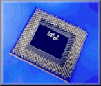
 Produced
in response to AMD’s announcement of a 533MHz K6-2, the Celeron 533 is no different
from the Celerons that have been around since the release of the 300A seemingly
ages ago.
The Celeron 533 is available only in a PPGA (Plastic Pin Grid Array) Socket-370 package which is a move that Intel made after the release of the Celeron 433. All Celerons released prior to the introduction of the Celeron 466 were available in either a 370-pin PPGA Socket-370 package or a 242-pin SEPP (Single Edge Processor Package) Slot-1 version.
However, the 466, 500, and now the 533 are all PPGA-only CPUs, meaning that you can only use them in Socket-370 motherboards or in Slot-1 motherboards by using a Socket-370 to Slot-1 converter card. Such cards have been manufactured by Iwill, MSI, ABIT and ASUS, among others.
 The
reason the move from Slot-1 to Socket-370 was made was because it’s simply cheaper
to produce a socketed CPU than it is to produce a CPU and plant it on a processor
card. The move was made possible because of the 128KB L2 cache that is integrated
into the die of the Celeron CPU itself, meaning that there was no reason to
have the processor card (it was originally used to house the 512KB of L2 cache
on the original Pentium II and Pentium III CPUs). The move to Socket-370 resulted
in an overall reduction of the street price of the Celeron CPU by around 15%,
which is very noticeable in spite of the fact that the CPUs retail for under
$100. When you’re dealing with a low-cost CPU, every dollar matters.
The Celeron 533, like all of the previous members of the Celeron family since the 300A is based on the 0.25-micron Mendocino core. What defines the Mendocino core is the lack of any SSE instructions, a full 128KB on-die L2 cache, and an on-die 32KB L1 cache split into 16KB data and 16KB instruction set caches. While the Celeron was originally supposed to gain SSE instructions as well as the use of the 100MHz FSB frequency in 2000, the lack of demand for a revamped Celeron and a simple desire from OEMs for a higher clock speed chip resulted in the production of the 533 as another 66MHz FSB Celeron based on the Mendocino core.
The Celeron 533 makes use of an extremely high 8.0x clock multiplier and officially runs on the 66MHz FSB. The 8.0x clock multiplier limits the overclocking potential of the CPU because increasing the FSB to 100MHz would result in an 800MHz frequency, a mark that the current yields on the Mendocino core isn’t capable of hitting in decent quantities.


0 Comments
View All Comments