i820 Motherboard Roundup - January 2000
by Anand Lal Shimpi on January 28, 2000 2:44 AM EST- Posted in
- Motherboards
Before diving into the motherboards we’ll want to take a quick glance at the i820 chipset itself. For more in-depth coverage of the i820 chipset feel free to take a look at our i820 Chipset Review.
The i820 chipset is the second chipset from Intel (if you count the i810 and i810E as being one chipset release) to make use of the Accelerated Hub Architecture (AHA). Intel’s AHA is the replacement for the age old system of splitting the core logic into bridges, most recently, into a North Bridge and a South Bridge.
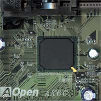
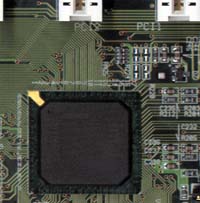
The i820’s AHA is split into three major parts, called hubs: the Memory Controller Hub (MCH), the I/O Controller Hub (ICH) and the Firmware Hub (FWH), which is merely a fancy name for the BIOS.
 The
MCH, as the name implies, provides the common interface between the processor,
AGP bus, and the memory bus. There are two versions of the MCH: the 82820 and
the 82820DP The latter is for use with dual processor motherboards, but since
they are both 324-pin, the solutions are interchangeable.
The
MCH, as the name implies, provides the common interface between the processor,
AGP bus, and the memory bus. There are two versions of the MCH: the 82820 and
the 82820DP The latter is for use with dual processor motherboards, but since
they are both 324-pin, the solutions are interchangeable.
From a memory standpoint, it acts as sort of a translator between the CPU and the memory bus. Although the 820’s MCH officially supports RDRAM, it’s implementation of RDRAM is a 16-bit wide implementation of the memory bus. And as we already know, the P6 bus provides a 64-bit data pathway to and from the CPU. So what happens when you want to send 64-bits of data from to a 16-bit wide memory bus?
This is where the MCH steps in and makes sure that the 64-bit wide CPU bus is effectively translated and piped down into the 16-bit wide memory bus. If you’ve ever heard anyone complaining about RDRAM’s increased latency versus SDRAM, you’re looking at one major cause for those complaints, the process of sending 64-bits of data down into a 16-bit data path. The MCH itself provides for this translation and, in doing so, obviously helps to produce the increased latency that we often complain about being associated with RDRAM.
This is why it is correct to state that the latency issues associated with RDRAM are actually best associated with the RDRAM implementation on the i820 chipset. There is always the possibility of having a wider memory bus with an RDRAM implementation thus helping to decrease the latencies associated with the 16-bit implementation on the i820 chipset.
The MCH also provides for the AGP 4X support of the i820 chipset. While the AGP 4X support doesn’t offer an incredible performance increase over the AGP 2X support that is present in the BX chipset, the biggest advantage the i820 chipset offers over previous Intel chipsets is its support for the ½ AGP clock divider.
By allowing for the AGP bus to operate at ½ the frequency of the system bus, the i820 chipset allows for official support for the 133MHz FSB and increases the overclocking potential of most systems since FSB frequencies above 133MHz can be picked without worrying too much about your AGP card not being able to handle the increased bus speed.
 The
801AA I/O Controller Hub (ICH) found on the i810 and i810E chipsets is also
a part of the i820 chipset. The 801AA is what drives the PCI bus on i820 motherboards,
and it supports up to 6 PCI slots. Notice that there is no mention of support
for ISA slots with the 801AA, the reason behind that is because the ICH does
not support any ISA slots. If motherboard manufacturers wish to include ISA
slots in their motherboard design then they will have to make use of an optional
ISA bridge that will take up valuable PCB space on the motherboard as well as
slightly increase the cost of the board.
The
801AA I/O Controller Hub (ICH) found on the i810 and i810E chipsets is also
a part of the i820 chipset. The 801AA is what drives the PCI bus on i820 motherboards,
and it supports up to 6 PCI slots. Notice that there is no mention of support
for ISA slots with the 801AA, the reason behind that is because the ICH does
not support any ISA slots. If motherboard manufacturers wish to include ISA
slots in their motherboard design then they will have to make use of an optional
ISA bridge that will take up valuable PCB space on the motherboard as well as
slightly increase the cost of the board.
From a peripheral standpoint, the 801AA is what allows i820 motherboards to boast native support for Ultra ATA 66 (4 devices allowed) as well as USB support (2 ports) and support for AMR (Audio Modem Riser) cards.


1 Comments
View All Comments
renterpoint - Wednesday, April 13, 2022 - link
This is a very nice motherboard. Thank you for posting such a nice piece of information.https://renterpoint.com/suv