Today’s Celeron is a little different than the Celerons that were around not too long ago. Ever since after the release of the Celeron 533, the Celeron has been manufactured using a different core. While everything prior to the Celeron 533A and the 566 had been manufactured using the 0.25-micron Mendocino core (128KB on-die L2, no SSE) the last few Celeron releases have been of processors that feature the new Coppermine128 core.
As we described in our original Celeron “Coppermine128” review, the main differences between the Coppermine128 core and the Mendocino core exist in the fact that the Coppermine128 core features the same SSE instructions that have been with the Pentium III since the Katmai core and it also features the same 256-bit data path to its L2 cache as the newer Pentium III “Coppermine” that it is derived from.
The Coppermine128 is manufactured by essentially taking a regular Pentium III based on the Coppermine core and disabling half of the L2 cache. This can be verified by looking at the die sizes for both the Coppermine128-based Celerons and the Coppermine Pentium IIIs (they are equal). The reason Intel does this is because there is no guarantee that when they produce a Pentium III with 256KB of L2 cache on-die that all of that 256KB L2 will be functional and fit for sale as a part of a processor. In the event that some of the 256KB L2 fails the required production tests, Intel can simply disable 1/2 of the L2 and re-label the part as a Celeron after changing the clock speed and FSB pins of the CPU.
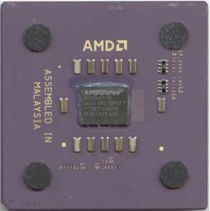
AMD's Duron
Now AMD goes about this problem in an entirely different way. They simply duplicate the number of L2 cache columns and if there is a particular block that fails production tests then AMD can simply disable the entire column. It is because of this that the Thunderbird and Duron are actually two different dies.
But let’s get back to the Celeron. Because the Celeron is basically a Coppermine core with 1/2 of the L2 cache disabled, the Celeron also loses half of the associativity of the Coppermine’s L2 cache, meaning the processor features a 4-way set associative L2 cache versus the 8-way set associative cache on the Pentium III. This actually hurts the Celeron more than you would think as it dramatically decreases the hit rate of the processor’s cache.
Combined with the fact that the Celeron is still limited by the 66MHz FSB and its 66MHz memory bus and you have a part that is significantly slower than an equivalently clocked Pentium III, Athlon, Duron or Thunderbird.
|
CPU
Specification Comparison
|
||||||||
|
AMD
Duron
|
AMD
Athlon
|
Intel
Pentium III
|
Intel
Celeron
|
|||||
| Core |
Spitfire
|
K7
|
K75
|
Thunderbird
|
Katmai
|
Coppermine
|
Mendocino
|
Coppermine128
|
|
Clock Speed |
600
- 700 MHz
|
500
- 700 MHz
|
750
- 1000 MHz*
|
450
- 600 MHz
|
500
- 1000 MHz
|
300
- 533 MHz
|
533
- 700 MHz
|
|
| L1 Cache |
128KB
|
32KB
|
||||||
| L2 Cache |
64KB
|
512KB
|
256KB
|
512KB
|
256KB
|
128KB
|
||
| L2 Cache speed |
core
clock
|
1/2
core
|
2/5
or 1/3 core
|
core
clock
|
1/2
core
|
core
clock
|
||
| L2 Cache bus |
64-bit
|
256-bit
|
64-bit
|
256-bit
|
||||
| System Bus |
100 MHz DDR (200 MHz effective) EV6
|
100
- 133 MHz GTL+
|
66
MHz GTL+
|
|||||
| Interface |
Socket-A
|
Slot-A
|
Socket-A
Slot-A (OEM only) |
Slot-1
|
Slot-1
Socket-370 |
Socket-370
|
||
| Manufacturing Process |
0.18
micron
|
0.25
micron
|
0.18
micron
|
0.25
micron
|
0.18
micron
|
0.25
micron
|
0.18
micron
|
|
| Die Size |
100mm^2
|
184
mm^2
|
102mm^2
|
120mm^2
|
128mm^2
|
106mm^2
|
153mm^2
|
106mm^2
|
| Transistor Count |
25
million
|
22
million
|
37
million
|
9.5
million
|
28
million
|
19
million
|
28
million
|
|
* Note: The K75 core actually took over the entire Athlon line and was available in 500 - 750MHz versions as well although it launched at 750MHz. The Thunderbird, although officially launched at 750MHz is available at speeds lower than 750MHz but only as OEM parts.


0 Comments
View All Comments