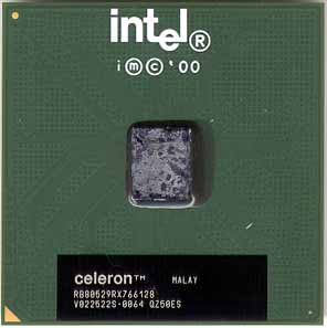
Budget CPU Upgrades: Intel's Celeron 766
by Anand Lal Shimpi on November 26, 2000 12:00 PM EST- Posted in
- CPUs
The Chip
The Celeron 766 remains unchanged from the previous Celeron processors. It is still manufactured by disabling half of the cache on low-yield Pentium IIIs that have bad cache blocks, thus giving the Celeron half the cache as well as making that cache half as associative as the Pentium III’s cache. This ends up hurting the Celeron severely as it, clock for clock, is unable to outperform the Pentium III, even when both are clocked at the same FSB/memory clock.
The explanation for this is simple, the less associative a processor’s cache is, the lower hit-rate it has, and the lower the hit rate, the more times the CPU has to go to main memory to fetch needed information. In the case of the Celeron, the memory bus is running at a horrendously slow 66MHz which just amplifies the downsides to its 4-way set associative L2 cache versus the Pentium III’s 8-way set associative L2. For more information on cache mapping techniques, check out our one page guide here.
Celeron 766 Specifications
· 0.18-micron Coppermine128 core
· 766MHz clock speed – 11.5x clock multiplier
· 32KB on-die L1 cache running at core speed
· 256-bit Advanced Transfer Cache – 4-way set associative 128KB on-die L2 cache running at core speed
· Advanced System Buffering
· 370-pin FC-PGA Socket-370 GTL+ CPU interface running at 66MHz
· 1.65v core voltage
The Celeron 700 is really no different from the 566/600MHz parts that have been on the streets for a while now. It is still based on the same 0.18-micron Coppermine128 core, features the same amount of L1 cache (16KB Instruction + 16KB Data cache) and the same 128KB inclusive L2 cache.
|
CPU
Specification Comparison
|
||||||||
| AMD Duron |
AMD
Athlon
|
Intel
Pentium III
|
Intel
Celeron
|
|||||
| Core |
Spitfire
|
K7
|
K75
|
Thunderbird
|
Katmai
|
Coppermine
|
Mendocino
|
Coppermine128
|
|
Clock Speed |
600
- 800 MHz
|
500
- 700 MHz
|
750
- 1000 MHz
|
750
- 1200 MHz
|
450
- 600 MHz
|
500
- 1000 MHz
|
300
- 533 MHz
|
533
- 766 MHz
|
| L1 Cache |
128KB
|
32KB
|
||||||
| L2 Cache |
64KB
|
512KB
|
256KB
|
512KB
|
256KB
|
128KB
|
||
| L2 Cache speed |
core
clock
|
1/2
core
|
2/5
or 1/3 core
|
core
clock
|
1/2
core
|
core
clock
|
||
| L2 Cache bus |
64-bit
|
256-bit
|
64-bit
|
256-bit
|
||||
| System Bus |
100 MHz DDR (200 MHz effective) EV6
|
100
- 133 MHz GTL+
|
66
MHz GTL+
|
|||||
| Interface |
Socket-A
|
Slot-A
|
Socket-A
Slot-A (OEM only up to 800MHz) |
Slot-1
|
Slot-1
Socket-370 |
Socket-370
|
||
| Manufacturing Process |
0.18
micron
|
0.25
micron
|
0.18
micron
|
0.25
micron
|
0.18
micron
|
0.25
micron
|
0.18
micron
|
|
| Die Size |
100mm^2
|
184
mm^2
|
102mm^2
|
120mm^2
|
128mm^2
|
106mm^2
|
153mm^2
|
106mm^2
|
| Transistor Count |
25
million
|
22
million
|
37
million
|
9.5
million
|
28
million
|
19
million
|
28
million
|
|


1 Comments
View All Comments
sunny123 - Sunday, June 30, 2019 - link
I am here and i can say you now just click here this site <a href="https://getrobloxfreerobux.com">robux generator free</a> then learn more about for this game.