Intel's E7500 Chipset: Dual Channel DDR for Xeon
by Anand Lal Shimpi on February 25, 2002 3:00 AM EST- Posted in
- CPUs
The Chipset
The E7500 chipset introduces a number of firsts for Intel, all of which are important because they can now become potential technology candidates for future desktop chipsets.
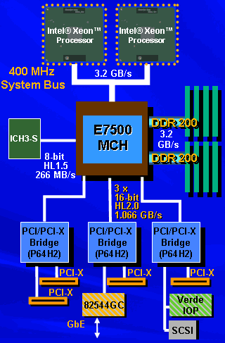
The E7500 Memory Controller Hub (MCH) obviously contains the bulk of the improvements that make the chipset what it is. First and foremost is the introduction of a dual channel (2 x 72-bit ECC) DDR SDRAM memory controller. The memory controller in the E7500 is validated for use with both DDR200 and DDR266 SDRAM however the bus will only operate at 100MHz (DDR200 speeds). This means that although you can use DDR266 SDRAM in it, your memory will always run at DDR200 speeds. Intel's reasoning behind this that dual DDR200 channels yield a theoretical 3.2GB/s of bandwidth to main memory which is perfectly matched up to the 3.2GB/s FSB. As we've seen in the past (take the KT133A chipset for example), a synchronized FSB and memory bus generally yields lower latency CPU/memory accesses than an asynchronous setup. It is very clear however that when Intel does move to a 133MHz (533MHz quad-pumped) FSB, a future successor to the E7500 chipset will support DDR266 SDRAM.
The E7500 MCH supports up to 16GB of DDR200 SDRAM through its 8 memory banks; but since it is a dual channel DDR SDRAM solution memory must be installed in pairs of two.
The I/O subsystem of the chipset is also improved with the introduction of Intel's first Hub-Link 2.0 interconnects. Intel first introduced their IHA (Intel Hub Architecture) with the i810 chipset as a replacement to the age-old North/South Bridge chipset architecture. The "hubs" as Intel likes to call them of a chipset were connected by a Hub Link interconnect that was essentially a high-speed serial bus. All current Intel chipsets still use the Hub Link 1.0 that was introduced with the i810, an 8-bit 133MHz double-pumped interconnect bus. The E7500 introduces the first Hub Link (HL) 1.5 and 2.0 buses used in an Intel chipset.
The E7500 features three HL 2.0 connections stemming from the MCH, each operating at 266MHz. Each HL 2.0 interconnect is 2-bytes wide (16-bits) thus resulting in a maximum of 1.06GB/s of bandwidth between the MCH and all devices attached to the bus. Since there are three HL 2.0 buses, a total of 3.2GB/s of I/O bandwidth is theoretically sustainable although reality will never come close to even matching that, much less exceeding it.
What purpose would these three HL 2.0 links serve? With most high-end server applications (e.g. database serving) demanding very high performance I/O subsystems including multidrive RAID arrays and Gigabit Ethernet, eating up bandwidth is a simple task. You'll find a number of E7500 platforms paired with Intel's P64H2 64-bit PCI/PCI-X controller which supports two 64-bit/133MHz PCI-X segments per controller. The P64H2 interfaces directly with HL 2.0 and thus a maximum of three of these chips can be used with an E7500 MCH, resulting in a maximum of six PCI/PCI-X buses. This type of I/O flexibility was previously only reserved for ServerWorks platforms but is greatly welcome and appreciated by the market in an Intel chipset.
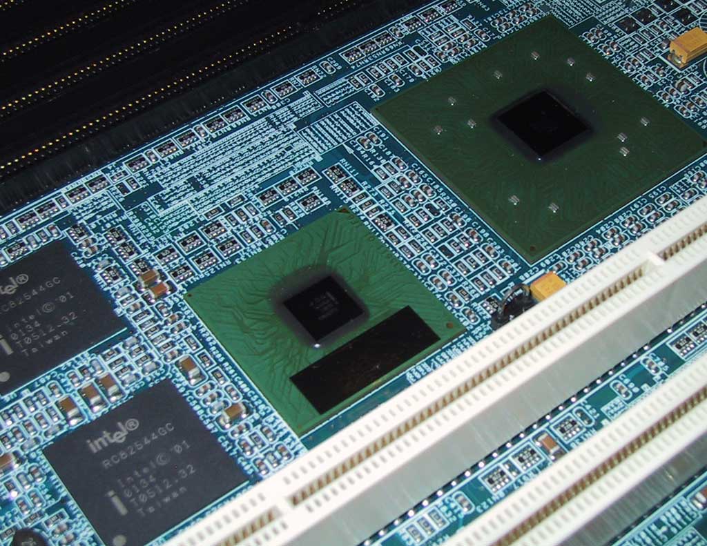
From left to right: Two Intel gigabit Ethernet controllers, P64H2 controller, E7500 MCH
To round things off, the E7500 features legacy support through its I/O Controller Hub (ICH). The ICH used with the E7500 is ICH3-S which works on a HL 1.5 link. The only difference between HL 1.5 and HL 1.0 is that it is electrically compatible with HL 2.0 which simplifies design and layout for motherboard manufacturers.


0 Comments
View All Comments