3DLabs' P10 Visual Processing Unit - When a CPU & GPU Collide
by Anand Lal Shimpi on May 3, 2002 7:30 AM EST- Posted in
- GPUs
VPU - It's Time to Learn a new Acronym
For 3DLabs, the term GPU has too negative of a connotation to use for their next-generation part. Current GPUs aren't flexible enough and thus when 3DLabs wanted to put a name to the face of their technology they came up with the term - Visual Processing Unit (VPU). The abbreviation is similar enough to CPU to properly convey its message while it's also different enough from GPU to signify a radically different approach to solving the problem.
The codename of 3DLabs' new part is called the P10; it's the first incarnation of what 3DLabs calls their Visual Processing architecture and its surely not going to be the last. However what makes the P10 VPU so different from the GeForce4's NV25 or the Radeon 8500's R200 isn't its pipeline; the same stages in the 3D pipeline still exist, it's what happens at each one of those stages that 3DLabs has set out to change.
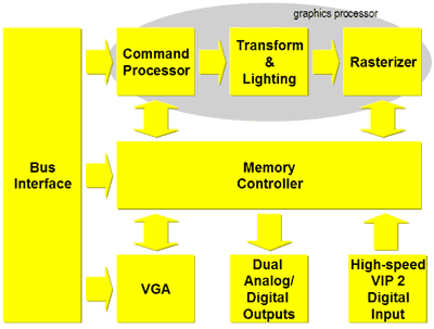
From a high-level you can see that the P10 isn't very different at all. The biggest improvement over the competition here is the use of a 256-bit DDR memory bus. The GeForce4 and Radeon 8500 both use a 128-bit DDR memory bus so this effectively doubles the peak theoretical memory bandwidth that can be attained. Because of the use of BGA memory it becomes easier to route traces making 256-bit DDR memory buses a reality for more than just 3DLabs, they're simply the first to introduce it. While 3DLabs hasn't released any card specs yet, they are claiming over 20GB/s of memory bandwidth is possible with the P10 meaning that they'd need at least 312.5MHz DDR SDRAM. Considering that the current GeForce4 Ti 4600 uses 325MHz DDR SDRAM, it's very possible that you'll see cards with over 20GB/s of memory bandwidth.
Other than the 256-bit memory bus and the addition of a block labeled as the Command Processor (which we'll get to later), the P10 looks pretty familiar; here are some quick specs:
- 0.15-micron manufacturing process (same process as the GeForce4)
- 76M transistors
- Fabbed at TSMC (NVIDIA's chips are made here as well)
- 860 ball HSBGA package (TSMC's latest packaging technology)
- 4 pixel rendering pipelines, can process two textures per pipeline
- 256-bit DDR memory interface (up to 20GB/s of memory bandwidth w/ 312.5MHz DDR)
- up to 256MB of memory on-board
- AGP 4X support
- Full DX8 pixel and vertex shader support
We've been deliberately light on the specs here as the rest must be explained in greater detail; it wouldn't do them justice to put them in a simple list.


0 Comments
View All Comments