The Qualcomm Snapdragon X Architecture Deep Dive: Getting To Know Oryon and Adreno X1
by Ryan Smith on June 13, 2024 9:00 AM ESTAdreno X1 GPU Architecture: A More Familiar Face
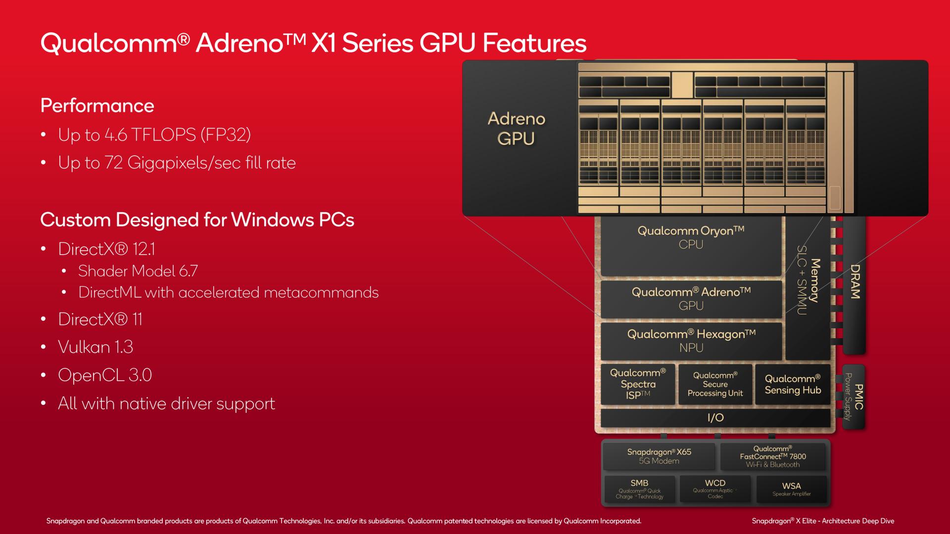
Shifting gears, let’s talk about the Snapdragon X SoC’s GPU architecture: Adreno X.
Unlike the Oryon CPU cores, Adreno X1 is not a wholly new hardware architecture. In fact, with 3 generations of 8cx SoCs before it, it’s not even new to Windows. Still, Qualcomm has been notoriously tight-lipped about their GPU architectures over the years, so the GPU architecture may as well be new to AnandTech readers. Suffice it to say, I’ve been trying to get a detailed disclosure from Qualcomm for over a decade at this point, and with Snapdragon X, they’re finally delivering.
At a high level, the Adreno X1 GPU architecture is the latest revision of Qualcomm’s ongoing series of Adreno architectures, with the X1 representing the 7th generation. Adreno itself is based on an acquisition from ATI over 15 years ago (Adreno is an anagram of Radeon), and over the years Qualcomm’s Adreno architecture has more often than not been the GPU to beat in the Android space.
Things are a bit different in the Windows space, of course, as discrete GPUs push integrated GPUs well off to the side for workloads that absolutely need high GPU performance. And because game development has never become fully divorced from GPU architectures/drivers, Qualcomm’s miniscule presence in the Windows market over the years has led to them going often overlooked by game developers. Still, Qualcomm isn’t new to the Windows game, which gives them a leg-up as they try to move into taking a larger share of the Windows market.
From a feature standpoint, the Adreno X1 GPU architecture is unfortunately a bit dated compared to contemporary x86 SoCs. While the architecture does support ray tracing, the chip isn’t able to support the full DirectX 12 Ultimate (feature level 12_2) feature set. And that means it must report itself to DirectX applications as a feature level 12_1 GPU, which means most games will restrict themselves to those features.
That said, Adreno X1 does support some advanced features, which are already being actively used on Android where DirectX’s feature levels do not exist. As previously noted, there is ray tracing support, and this is exposed on Windows applications via the Vulkan API and its ray query calls. Given how limited Vulkan use is on Windows, Qualcomm understandably doesn’t go into the subject in too much depth; but it sounds like Qualcomm’s implementation is a level 2 design with hardware ray testing but no hardware BVH processing, which would make it similar in scope to AMD’s RDNA2 architecture.
| DirectX 12 Feature Levels | |||||
| 12_2 (DX12 Ult.) |
12_1 | 12_0 | |||
| Ray Tracing (DXR 1.1) |
Yes | No | No | ||
| Variable Rate Shading (Tier 2) |
Yes | No | No | ||
| Mesh Shaders | Yes | No | No | ||
| Sampler Feedback | Yes | No | No | ||
| Conservative Rasterization | Yes | Yes | No | ||
| Raster Order Views | Yes | Yes | No | ||
| Tiled Resources (Tier 2) |
Yes | Yes | Yes | ||
| Bindless Resources (Tier 2) |
Yes | Yes | Yes | ||
| Typed UAV Load | Yes | Yes | Yes | ||
Otherwise, variable rate shading (VRS) tier 2 is supported as well, which is critical for optimizing shader workloads on mobile GPUs. So it appears the missing features holding the X1 back from DirectX 12 Ultimate support are mesh shaders and sampler feedback, which are admittedly some pretty big hardware changes.
In terms of API support, as previously noted, the Adreno X1 GPU supports DirectX and Vulkan. Qualcomm offers native drivers/paths for DirectX 12 and DirectX 11, Vulkan 1.3, and OpenCL 3.0. The only notable exception here is DirectX 9 support, which like fellow SoC vendor Intel, is implemented using D3D9on12, Microsoft's mapping layer for translating DX9 commands to DX12. DX9 games are far and few these days (the API was supplanted by DX10/11 over 15 years ago), but since this is Windows, backwards compatibility is an ongoing expectation.
Conversely, on the compute front Microsoft’s new DirectML API for low-level GPU access for machine learning is supported. Qualcomm even has optimized metacommands written for the GPU, so that software tapping into DirectML can run more efficiently without knowing anything else about the architecture.
Adreno X1 GPU Architecture In Depth
High-level functionality aside, let’s take a look at the low-level architecture.
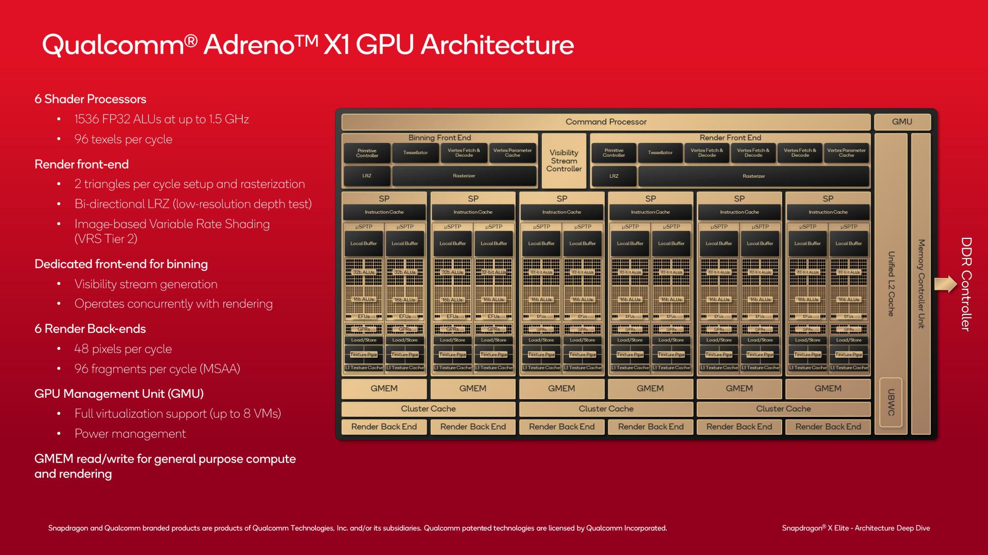
The Adreno X1 GPU is split up into 6 shader processor (SP) blocks, each offering 256 FP32 ALUs for a total of 1536 ALUs. With a peak clockspeed of 1.5GHz, this gives the integrated GPU on Snapdragon X a maximum throughput of 4.6 TFLOPS (with lesser amounts for lower-end SKUs).
Split up into the traditional front-end/SP/back-end setup we see with other GPUs, the front-end of the GPU handles triangle setup and rasterization, as well as binning for the GPU’s tile-based rendering mode. Of note, the GPU front-end can setup and raster 2 tringles per clock, which is not going to turn any heads in the PC space in 2024, but is respectable for an integrated GPU. Boosting its performance, the front-end can also do early depth testing to reject polygons that will never be visible before they are even rasterized.
Meanwhile the back-end is made from 6 render output units (ROPs), which can process 8 pixels per cycle each, for a total of 48 pixels/clock rendered. The render back-ends are plugged in to a local cache, as well as an important scratchpad memory that Qualcomm calls GMEM (more on this in a bit).
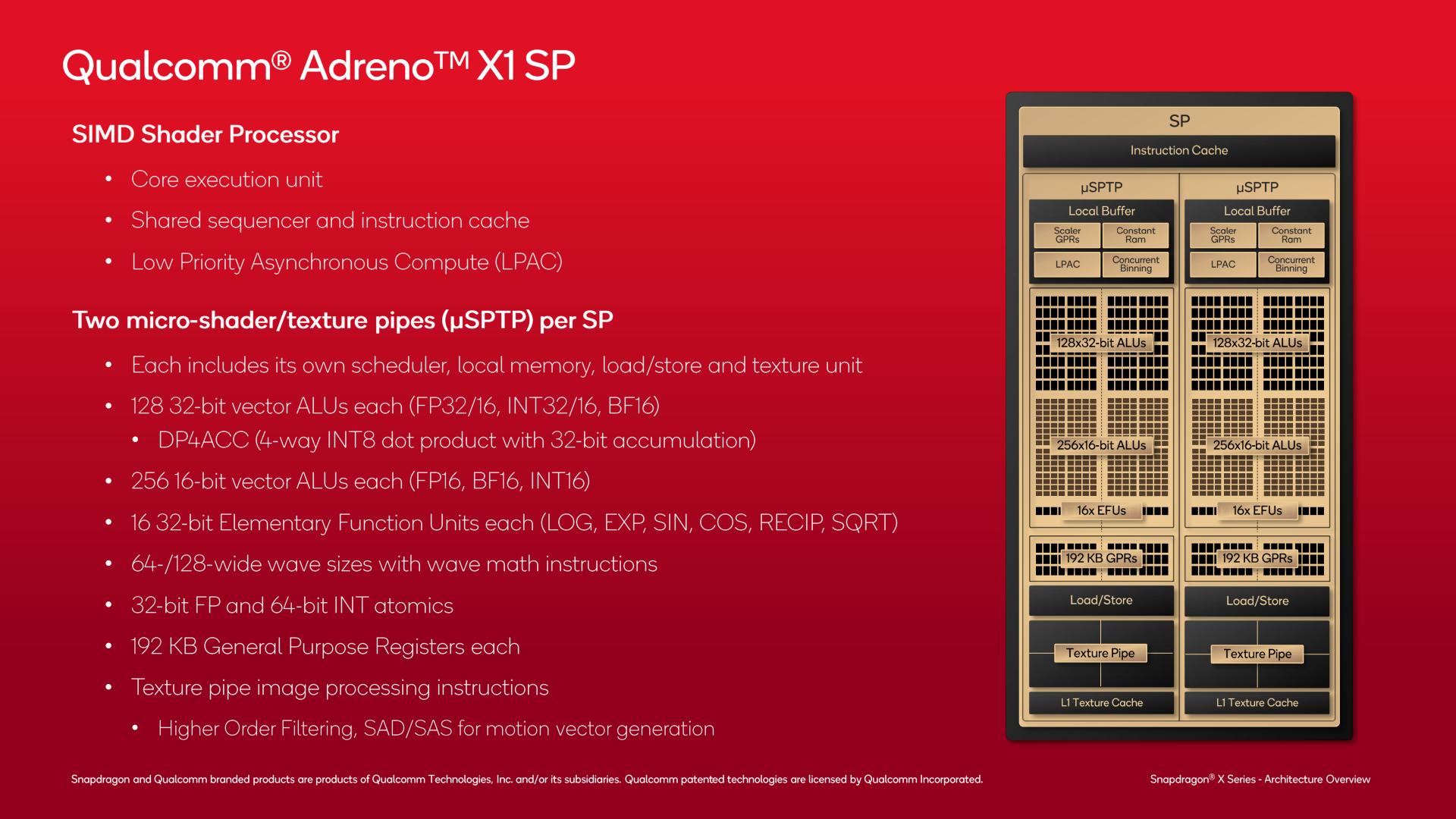
The individual shader processor blocks themselves are relatively customary, especially if you’ve seen an NVIDIA GPU architecture diagram. Each SP is further subdivided into two micro-pipes (micro shader pipe texture pipe, or uSPTP), which is helmed by its own dedicated scheduler and other resources such as local memory, load/store units, and texture units.
Each uSPTP offers 128 FP32 ALUs. And, in a bit of a surprise, there is also a separate set of 256 FP16 ALUs, meaning that Adreno X1 doesn’t have to share resources when processing FP16 and FP32 data, unlike architectures which execute FP16 operations on FP32 ALUs. Though for good measure, the FP32 units can be used for FP16 operations as well, if the GPU scheduler determines it’s needed.
Finally, there are 16 elementary functional units (EFUs), which handle transcendental functions such as LOG, SQRT, and other rare (but important) mathematical functions.
Surprisingly here, the Adreno X1 uses a rather large wavefront size. Depending on the mode, Qualcomm uses either 64 or 128 lane wide waves, with Qualcomm telling us that they typically use 128-wide wavefronts for 16bit operations such as fragment shaders, while 64-wide wavefronts are used for 32bit operations (e.g. pixel shaders).
Comparatively, AMD’s RDNA architectures use 32/64 wide wavefronts, and NVIDIA’s wavefronts/warps are always 32 wide. Wide designs have fallen out of favor in the PC space due to the difficulty in keeping them fed (too much divergence), so this is interesting to see. Ultimately, despite the usual wavefront size concerns, it seems to be working well for Qualcomm given the high GPU performance of their smartphone SoCs – no small feat given the high resolution of phone screens.
ALUs aside, each uSPTP includes their own texture units, which are capable of spitting out 8 texels per clock per uSPTP. There’s also limited image processing functionality here, including texture filtering, and even SAD/SAS instructions for generating motion vectors.
Finally, there’s quite a bit of register space within each uSPTP. Along with the L1 texture cache, there’s a total of 192KB of general purpose registers to keep the various blocks fed and to try to hide latency bubbles in the wavefronts.
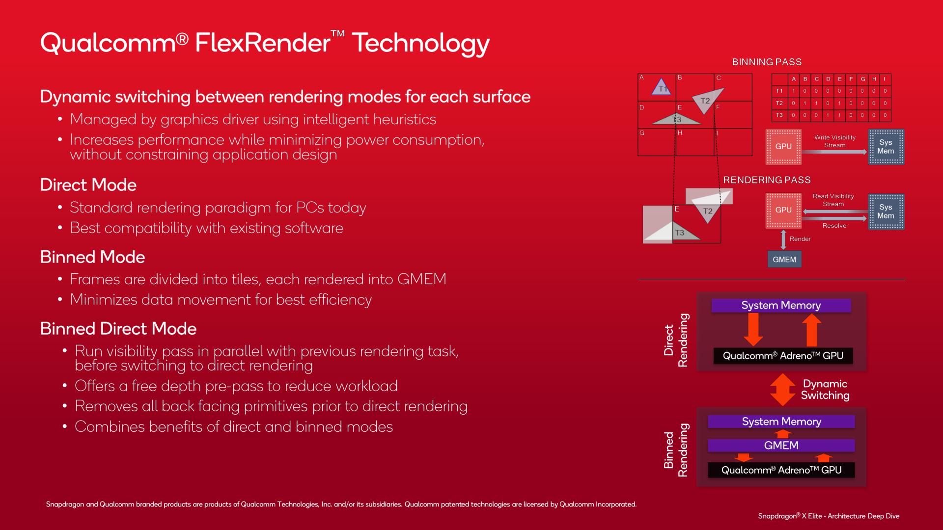
As noted earlier, the Adreno X1 supports multiple rendering modes in order to get the best performance possible, which the company calls their FlexRender technology. This is a subject that doesn’t come up too often with PC GPU designs, but is of greater importance in the mobile space for historical and efficiency reasons.
Besides the traditional direct/immediate mode rendering method (the typical mode for most PC GPUs), Qualcomm also supports tile-based rendering, which they call binned mode. As with other tile-based renderers, binned mode splits a screen up into multiple tiles, and then renders each one separately. This allows the GPU to only work on a subset of data at once, keeping most of that data in its local caches and minimizing the amount of traffic that goes to DRAM, which is both power-expensive and performance-constricting.
And finally, Adreno X1 has a third mode that combines the best of binned and direct rendering, which they call binned direct mode. This mode runs a binned visibility pass before switching to direct rendering, as a means to further cull back-facing (non-visible) triangles so that they don’t get rastered. Only after that data is culled does the GPU then switch over to direct rendering mode, now with a reduced workload.
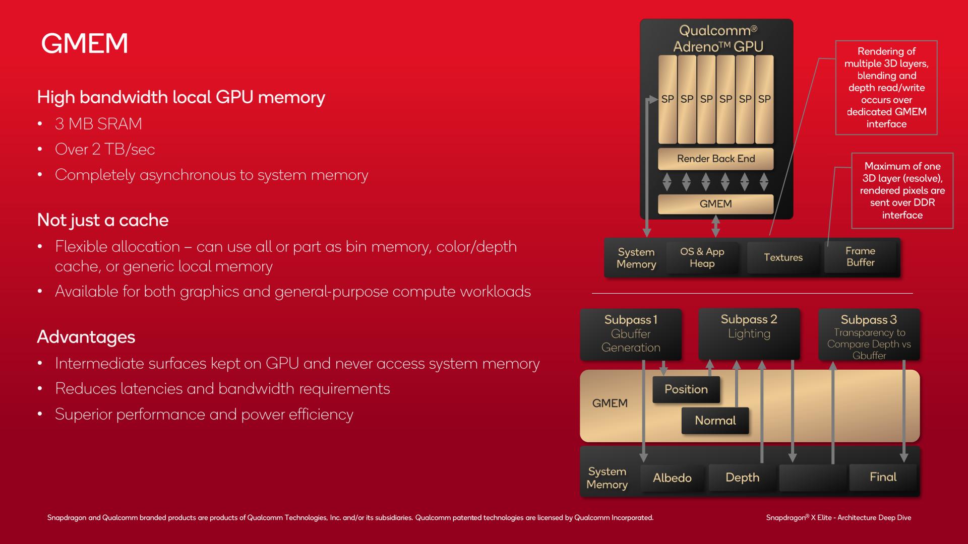
Key to making the binned rendering modes work is the GPU’s GMEM, a 3MB SRAM block that serves as a very high bandwidth scratch pad for the GPU. Architecturally, GMEM is more than a cache, as it’s decoupled from the system memory hierarchy, and the GPU can do virtually anything it wants with the memory (including using it as a cache, if need be).
At 3MB in size, the GMEM block is not very large overall. But that’s big enough to store a tile – and thus prevent a whole lot of traffic from hitting the system memory. And it’s fast, too, with 2.3TB/second of bandwidth, which is enough bandwidth to allow the ROPs to run at full-tilt without being constrained by memory bandwidth.
With the GMEM block in place, in an ideal scenario, the GPU only needs to write out to the DRAM once per title, when it finishes rendering said tile. In practice, of course, there ends up being more DRAM traffic than that, but this is one of Qualcomm’s key features for avoiding chewing up memory bandwidth and power with GPU writes to DRAM.
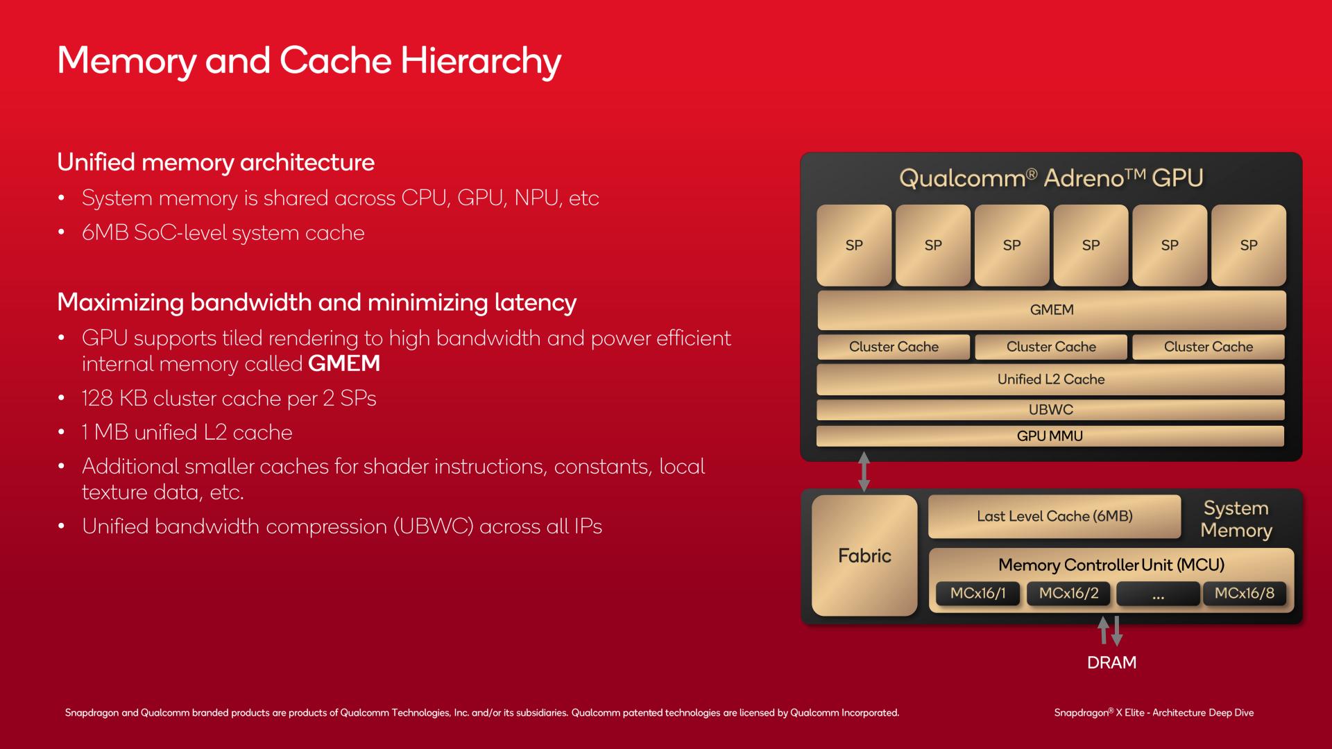
And when the Adreno X1 does need to go to system memory, it will go through its own remaining caches, before finally reaching the Snapdragon X’s shared memory controller.
Above the GMEM, there is a 128KB cluster cache for each pair of SPs (for 384KB in total for a full Snapdragon X). And above that still is a 1MB unified L2 cache for the GPU.
Finally, this leaves the system level cache (L3/SLC), which serves all of the processing blocks on the GPU. And when all else fails, there is the DRAM.
On a concluding note, while Qualcomm doesn’t have a dedicated slide for this, it’s interesting to note that the Adreno X1 GPU also includes a dedicated RISC controller within the GPU which serves as a GPU Management Unit (GMU). The GMU provides several features, the most important of which is power management within the GPU. The GMU works in concert with power management requests elsewhere in the SoC, allowing the chip to reallocate power between the different blocks depending on what the SoC decides is the most performant allocation method.


51 Comments
View All Comments
skavi - Friday, June 14, 2024 - link
great article. it’s nice to see quality stuff like this. Replynandnandnand - Friday, June 14, 2024 - link
"Officially, Qualcomm isn’t assigning any TDP ratings to these chip SKUs, as, in principle, any given SKU can be used across the entire spectrum of power levels."A Qualcope since they are differentiating the SKUs by max turbo clocks. Reply
eastcoast_pete - Friday, June 14, 2024 - link
First, thanks Ryan! Glad to see you doing deep dives again.Questions: 1. Anything known about if and how well the Snapdragon Extreme would pair up with a dGPU? The iGPU's performance is (apparently) in the same ballpark as the 780M and the ARC in Meteor Lake, but gaming or workstation use would require a dGPU like a 4080 mobile Ada or the pro variant. So, any word from Qualcomm on playing nice with dGPUs?
2. The elephant in the room on the ARM side is the unresolved legal dispute between Qualcomm and ARM over whether Qualcomm has the right to use the cores developed (under an ALA) by Nuvia for the development of ARM-based cores for server CPUs in (now) client SoCs. Any news on that? Some writers have speculated that this uncertainty is one, maybe the key reason for Microsoft to also encourage Nvidia and MediaTek to develop client SoCs based on stock ARM architecture. MS might hedge its bets here, so they don't put all the work (and PR) into developing Windows-on ARM and "AI" everywhere and find themselves with no ARM Laptops available to customers if ARM prevails in court. Reply
Ryan Smith - Friday, June 14, 2024 - link
1) That question isn't really being entertained right now since the required software does not exist. If and when NVIDIA has a ARMv8 Windows driver set, then maybe we can get some answers.2) The Arm vs. Qualcomm legal dispute is ongoing. The court case itself doesn't start until late this year. In the meantime, any negotiations between QC and Arm would be taking place in private. There's not really much to say until that case either reaches its conclusion - at which point Arm could ask for various forms of injunctive relief - or the two companies come to an out-of-court settlement. Reply
eastcoast_pete - Saturday, June 15, 2024 - link
Thanks Ryan! Looking forward to the first tests. Replycontinuum - Saturday, June 15, 2024 - link
Great article, can't wait til actual reviews next week. Thanks Ryan! ReplyMooseMuffin - Saturday, June 15, 2024 - link
When should we expect to see Oryon cores in android phones? ReplyRyan Smith - Sunday, June 16, 2024 - link
Snapdragon 8 Gen 4 late this year. Replyabufrejoval - Thursday, June 20, 2024 - link
So the embargos have lifted......and the silence is deafening?
Is this Microsoft's Vision Pro moment? Reply
eastcoast_pete - Monday, June 24, 2024 - link
Sure looks like it. Copilot and Recall are a potential privacy and confidentiality nightmare (MS has promised/threatened it can remember pretty much anything); and the integration of "AI" into something that is actually useful remains elusive. I am a bit surprised that Qualcomm hasn't taken up some of that slack. For an example of useful AI-supported functionality: On at least some smartphones (Pixel, Samsung's Galaxy S24 models) one can get pretty good instant translation and transcription, and do so offline (!); no phoning home to the mothership required. But, that uses Google's software, so it's not coming to a Microsoft device near you or me anytime soon. Something like that in Windows, but with demonstrably lower power consumption than doing so on the CPU or GPU would show some value an NPU could bring. Absent that, the silence out of Redmond is indeed deafening. Reply