Original Link: https://www.anandtech.com/show/1056
For the longest time we’ve been pushing AMD to open up a bit and talk about more than their roadmaps and upcoming processors. When Intel breaks the 10GHz barrier with an air-cooled ALU or when they produce a 52Mbit SRAM on a 90nm wafer, we definitely hear about it. But when AMD does something incredible it remains confined to the walls of AMD R&D, tucked away in a beautiful part of eastern Germany – Dresden. So you can understand the surprise when AMD asked us to come and take a tour of their Dresden facilities and talk a bit about AMD’s technology and their direction.
Obviously not an opportunity to pass up, we hopped on a plane and made the journey to the 10F weather of Dresden, Germany. AMD’s influence on the area is clear; it isn’t often that public street signs carry the name of a company, but in the case of Dresden you will find that the same signs that direct you to the airport will also tell you how to get to AMD. The Dresden community is very grateful to AMD for the over 2,000 jobs created by AMD Saxony Manufacturing GmbH (the name given to AMD’s Fab 30 and their Dresden Design Center), especially since over 90% of those jobs were filled by East German residents.

Welcome to snowy Dresden
There’s very little known publicly about AMD’s advanced manufacturing plant in Dresden, other than what comes out of it and its name – Fab 30. As you’ve undoubtedly heard time and time again, the name Fab 30 comes from the age of AMD when the fab began mass production. AMD was founded in 1969 and the Dresden Fab began mass production in 1999 thus covering 30 years, which is where the ‘30’ in Fab 30 comes from.
What goes on in Dresden?
AMD’s Fab 30 was the home of the first Athlon processors to use Copper interconnects and it will be the exclusive home of Athlon 64 and Opteron processors upon their launch. Fab 30 started out as a 0.18-micron manufacturing facility but as of Q4 2002 has completely transitioned to manufacturing 0.13-micron parts, exclusively. AMD will continue to manufacture only 200mm wafers (8”) in Dresden but the plant will transition to 90nm manufacturing in 2004. With AMD’s CPUs in 2003 being manufactured out of Fab 30, that leaves Fab 25 in Austin to handle the production of flash memory.
As we mentioned in the introduction, AMD Saxony is more than just Fab 30, it also encompasses AMD’s Dresden Design Center (DDC). The Dresden Design Center was started as AMD’s focus for chipset design, but now that their task is almost complete the DDC will shift to handling AMD’s PCS (Personal Connectivity Solutions) devices. The DDC’s concluding task at this point is the development of AMD’s 8th generation chipset logic, primarily the enabling chipsets for Athlon 64 and Opteron. With AMD’s 8000 series development complete and strong industry support to continue to develop future Athlon 64/Opteron chipsets, AMD can shift the focus of the DDC to other things.
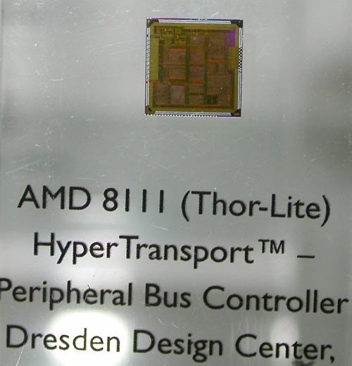
AMD's 8111 South Bridge designed in the DDC
The combination of the Fab and the Dresden Design Center (DDC) was said to require a $2.3 billion investment, with close to $2B already spent and the remaining $300M due to be used by the end of 2003. For an advanced microprocessor fabrication facility like Fab 30 this is the going rate for start-up costs, which is a major part of the reason why there are only two big competitors in the desktop CPU market; with such high barriers to entry, it’s very difficult to become a mass market competitor in the CPU business.
A Quick Tour through Fab 30
As we mentioned earlier, getting AMD to open up the doors of Fab 30 was almost unheard of and thus we did not expect to be able to talk about, much less see anything on our tour. Thankfully we were given a short but very informative tour through a part of AMD’s manufacturing that you rarely hear about – the Materials Analysis Labs. Because of AMD’s strict policies we were not able to bring you any pictures from within Fab 30, but we’ll try our best to describe exactly what we saw in words.

A picture outside Fab 30 as we left in the snow, this was the farthest inside
we could use our camera
You often hear about manufacturing yields and improving them, but very rarely do you get an idea of all of the work that goes into the actual process of improving them. Before we can explain how AMD’s Material Analysis Labs contribute to improving yields at Fab 30, you have to have a good understanding of exactly what improving yields means for AMD.
Obviously the higher AMD’s yields the more CPUs they can ship and the faster their CPUs can potentially be, but AMD’s own Ehrenfried Zschech had a much better way of explaining it. If the yields at Fab 30 were to drop 10% for just 8 hours, the drop in yield would cost AMD a cool $1 million. And remember we’re only talking about yields dropping for a matter of hours, if the defects causing the yields to decrease aren’t found and eliminated the loss could be devastating. Manufacturing yields are the life line of any fab-based microprocessor manufacturer, and considering the bullish comments from AMD on their yields at Fab 30 it worked out very well that we’re able to take you through some of the “how” behind detecting defects and turning them around into a way of improving yields.
The Materials Analysis Labs have two major tasks – to find defects and then to analyze them. The discovery of defects takes us to the Sample Preparation Lab, where silicon wafers are sent for defect detection and then prepped for analysis by the Materials Analysis Labs.
The wafers are sent from manufacturing to the Sample Preparation Lab along with a sheet of paper that contains information on what tests the folks in manufacturing want run on the wafers. What inspires manufacturing to suspect something has gone awry with the process and ship a wafer here? If there are any changes in yield, sudden or not, it is time to get to the bottom of why. Remember those calculations from before, a 10% drop in yield for just 8 hours costs $1M; we’re not talking about small sums of money here.
Once the wafers are in the hands of the engineers in AMD’s Sample Preparation Lab they are cut, polished and individual cores can be isolated if necessary. The Lab also can “decorate” wafers in order to make certain structures within the silicon more visible, which helps in the Materials Analysis Labs later on.
The wafers that make it to the Sample Preparation Lab aren’t necessarily made up of fully functional CPUs, in fact they are usually test structures. A test wafer is made up of a number of chips just like a mass production wafer, but instead of the chips being individual CPU cores the test wafer has a set of test structures printed on the wafer itself. The test structures can be lots of gates or an incredible amount of vias (vias are tiny wires that connect the various layers of a CPU) in order to stress the manufacturing process. Improving the yield on these test wafers directly improves the yield on producing actual CPUs, the test structures simply make for better test candidates.
The Sample Preparation Lab gets about 2 to 3 new defects to analyze per month, but what’s interesting to note is that not all of these defects influence yield. Granted there are some defects that will lower production yields but there are others that are simply smaller pieces of a much larger puzzle, and resolving those defects will pave the way for bigger defects to be taken care of.
Although it may not seem all that exciting, the work that goes on in the Sample Preparation Lab is critical to the defect analysis and fine tuning of AMD’s manufacturing process. Without good samples to work with, the engineers in the Materials Analysis Lab can’t produce any good results with which to diagnose defects. As one AMD employee put it, preparing the samples is 80% of the equation; now let’s take a look at the remaining 20%.
Welcome to the Materials Analysis Labs
Once the defective wafers are prepared in the Sample Preparation Lab they are sent to the Materials Analysis Labs where the actual analysis begins.
To give you an idea of the sensitivity of the equipment used in the Materials Analysis Labs, AMD had to build the entire set of Labs on a separate slab of concrete at Fab 30; the reason for this was to prevent minute vibrations from the rest of the facility to make their way into the Materials Analysis Labs (MALabs). The tools used in the MALabs are used for looking at pieces of silicon at atomic levels; any foreign vibrations could seriously impact the accuracy of the equipment.
The first part of the MALabs we walked through was the Transmission Electron Microscopy Lab – home to AMD’s highest resolution microscope. This lab is able to use a number of multimillion dollar microscopes to see individual Silicon atoms. The lab is quite useful in seeing differences in very thin layers such as the gate oxide in transistors. To give you an idea of how thin the gate oxide of current generation transistors happens to be, we’re talking about a thickness of around 1.2nm or approximately 5 atoms.
The purpose of these powerful microscopes is to more closely investigate defects in areas such as the gate oxide and thus can be used to improve the manufacturing processes.
Our next stop took us into the Scanning Electron Microscopy Lab, which is yet another high powered microscope lab but this time it is more focused on checking the dimensions of structures to make sure the manufacturing tools are in specification. The purpose of the Scanning Electron Microscopy Lab is to analyze defects, which was the major theme behind our tour at Fab 30. The tools within this lab can scan entire 8” wafers that are produced in the fab, once again mostly test structures.
One test that is run in the Scanning Electron Microscopy Lab is for Electron BackScatter Diffraction (EBSD) patterns. The way the test works is relatively simple in principle; a machine will bombard a copper interconnect line with electrons, and the diffraction pattern that results from the electrons bouncing off the line will give an indication of the grain of the copper. Over the past couple of days in Dresden we become intimately familiar with the importance of the grain of the copper wires to the reliability and performance of AMD’s processors.
Fab 30 – First to Copper, Now first to SOI
As you may remember, Fab 30 migrated to Copper interconnects very early on, even before Intel. The first CPUs to use the new Copper interconnects were actually engineering sample K6-2 processors, but they never made it onto the market. Just two months later, AMD began producing Thunderbird cores using Copper interconnects. It wasn’t until the Pentium 4 that Intel shifted to Copper interconnects, but truthfully it wasn’t necessary until the Pentium 4 for Intel. For AMD, Copper interconnects became an absolute requirement after their transition to the 0.13-micron Thoroughbred core although there were measurable improvements on previous processors.
The reason behind moving to Copper is often quoted as being the lower resistivity of Copper in comparison to Aluminum, but there are also other driving factors behind the move. With the move to Copper AMD was able to move to Inlaid Interconnects, which made lithography easier and avoided metal etching. Going deeper into the benefits of inlaid interconnects is beyond the scope of this article but the point to take away is that there are more drivers behind the move to Copper interconnects than lowering the inherent resistances of the wires.
Once again we find AMD breaking new ground at Fab 30 with their Hammer line of processors slated to be the first x86 CPUs to be manufactured using Partially Depleted Silicon on Insulator transistors. While both AMD and Intel are working towards introducing Fully Depleted SOI in a matter of years, only AMD is introducing PD-SOI. We’ve outlined the benefits of PD-SOI before but to recap, the end result are transistors that are much more efficient with current resulting in cooler running chips and the ability to scale to higher clock speeds.
We asked some of the AMD fab engineers how the move to SOI impacted yields and development time on Hammer. According to the AMD engineers, the move to SOI simply impacted the initial design stages but once that was taken care of the manufacturing was just like any other CPU to come out of Fab 30 – but obviously on SOI wafers.
With our questions about SOI’s impact on Hammer’s production we led into a series of questions about the highly anticipated processor release from AMD…
Updates on Hammer
Although Fab 30 will be initially the only place AMD manufactures their Athlon 64 and Opteron processors, it’s worth mentioning that Hammer CPUs weren’t scattered all over the place at the fab. Remember that Fab 30 is first and foremost a manufacturing facility, and the actual packaging and assembly is done off-shore so at most we could find wafers of Hammer cores but nothing more.
The testing and validation labs in the US are where you’re more likely to find fully functional Hammer systems, which is expected but still funny considering that Fab 30 is where the chip is being made and there are so few of them floating around.
With the launch of Hammer a quarter away at most, AMD has already begun producing final silicon out of Fab 30. As they mentioned to us during our time at the plant, it takes approximately three months of leadtime in order to regularly crank out the CPUs so Hammer production began at the very end of last year.
We also tried to get some more clarification involving the delay of Hammer, as it did not seem to be related to manufacturing issues. If you take into account the die size differences between Hammer and Athlon XP and compare the yields, currently Hammer is yielding just as high as the 0.13-micron Athlon XP CPUs and apparently yields have not really been a problem during the Hammer production process. Instead, AMD reiterated that the reason for the delay in the CPU’s launch was the performance and design of the part. Once all of the performance issues were hammered out (no pun intended) and the design was finalized then AMD was able to crank it up a notch and work towards the final stretch before the CPU’s release. Hammer’s design being the cause of the delays makes a lot of sense considering that AMD’s 0.13-micron process has been in action for a decent amount of time now, and manufacturing a 0.13-micron SOI Hammer and a 0.13-micron Thoroughbred are apparently very similar.
With yields high, production ramping up and strong support from their partners – it seems as if Hammer is finally ready for its debut. The motherboards and chipsets are quite stable and with final CPU silicon being produced the only question that remains is how fast the first CPUs will be. At Comdex last year AMD had a handful of Athlon 64s running at 1.8GHz and they’ve been targeting a ~2GHz launch all along, it will be interesting to see how much farther above 2GHz AMD is able to hit by the time the CPU launches. From what we’ve seen, a 2GHz Athlon 64 will definitely be competitive with Intel’s 3.06GHz Pentium 4 but at this point the market is expecting as much as possible from AMD.
Final Words
We hope you enjoyed this brief but rare look behind the scenes at AMD, and we hope this will be the first of many similar stories on Inside AMD here on AnandTech. We’ve expressed great interest in coming back to Dresden to spend some more time with the engineers and equipment at Fab 30 to bring you a more detailed picture of AMD’s capabilities as a microprocessor manufacturer.
There is one thing that’s for sure; AMD has not done a very good job of telling the public exactly what they’re capable of from a manufacturing standpoint. Intel has been talking about their manufacturing capabilities for quite some time now and has left the market with the impression that they are the only leader in the x86 manufacturing world. It is a shame because in reality, AMD has quite a few accomplishments of their own to talk about but it’s just a matter of getting them to loosen up and let you all in.
Fab 30 was nothing short of impressive; much more impressive than we had imagined before ever setting foot on the campus of AMD Saxony. The technology and engineering talent at Fab 30 can rival even that of Intel, but obviously on a smaller scale. Fab 30 will begin its transition to 90nm by the end of this year but mass production will not commence until next year, which will put them behind Intel’s schedule. AMD doesn’t have the plethora of manufacturing facilities that Intel does but with that said, Fab 30 can definitely hold its own among the more impressive production plants out there.
We would have liked to bring you more pictures and details from Fab 30 to truly show you the things that impressed us about AMD’s gold mine in Dresden, but that will have to wait for another time. Don’t worry, we’re working on getting AMD to let us tell and show more about what goes on behind the scenes. If you’ll remember from a few years back, it took Intel a while to open up but it eventually happened; AMD will be no different, it’s only a matter of time.
Be sure to check out the other articles in our Inside series:


