Original Link: https://www.anandtech.com/show/2139
AMD's 65nm Preview Part 2 - The Plot Thickens (Updated with Information from AMD)
by Anand Lal Shimpi on December 21, 2006 12:12 AM EST- Posted in
- CPUs
Updated: Page 3 has been updated to include an official AMD response on the Brisbane performance issues we've been seeing. AMD confirmed an increase in L2 cache latency in order to support a move to larger cache sizes in the future, which may or may not happen. The rest of the article remains unchanged.
Last week AMD sent us samples of its first 65nm processors, codenamed Brisbane, and it was a step towards being competitive with Intel again. The 65nm shrink yielded AMD's most efficient desktop processor to date, but it's still a far cry away from what Intel is able to accomplish with its Core 2 processors.
Although they won't be available until sometime next year, a closer look at AMD's 65nm lineup reveals an interesting fact. Until recently, AMD would differentiate between subsequent model numbers by clock speed and cache size, alternating between the two. So while the Athlon 64 X2 4600+ and 4800+ both ran at 2.4GHz, the latter had twice the L2 cache per core at 1MB. After Intel's Core 2 launch, AMD killed all non-FX 1MB L2 parts, resulting in a processor lineup that was mostly segregated according to clock speed. (Of course they then added the X2 5200+ and 5600+ back into the mix....) With the move to 65nm, AMD is once again introducing model numbers that it had killed off before, but without playing with L2 cache sizes; instead, AMD is breaking with recent tradition and implementing non-integer clock multipliers for these "new" in-between speeds. The table below explains it all:
| CPU | Clock Multiplier | Clock Speed |
| AMD Athlon 64 X2 5000+ EE | 13.0x | 2.6GHz |
| AMD Athlon 64 X2 4800+ EE | 12.5x | 2.5GHz |
| AMD Athlon 64 X2 4600+ EE | 12.0x | 2.4GHz |
| AMD Athlon 64 4400+ EE | 11.5x | 2.3GHz |
| AMD Athlon 64 X2 4000+ EE | 10.5x | 2.1GHz |
We didn't mention this in the original article, but all of AMD's 65nm CPUs are considered to be Energy Efficient (denoted by the letters EE in the table above). With its 90nm chips, AMD specifically selected lower voltage parts to be labeled as Energy Efficient, but right now all 65nm parts are. For the sake of simplicity, especially as we compare to older EE parts, we will simply refer to these chips as 65nm chips.
Note that the 65nm 4800+, 4400+ and 4000+ all use non-integer clock multipliers, a first for the Athlon 64 line. The implications for the end user are relatively minor, although it does mean that the model numbers will translate into more consistent performance graduations. In the past, having two chips running at the same clock speed but with different cache sizes meant that one would be faster only in those applications that could use the extra cache.
Despite support for non-integer clock multipliers, all AMD chips still only support integer memory dividers, meaning that only CPUs with even CPU multipliers can run at DDR2-800. All odd clocked (5000+) and half-clocked processors (4800+, 4400+, 4000+) run at a slower than DDR2-800 speed, even when set to DDR2-800 in the BIOS. AMD wouldn't discuss whether or not this would be addressed in the future, but if it is we'd have to wait for at least another silicon revision.
By now, none of this is new information, which brings us to why we're here today. In our original 65nm article we noticed a performance disparity between AMD's 65nm and 90nm processors, yet we had no official response from AMD as to why; today we have that answer. At the same time, we wanted to take a look at one of the half-multiplier chips and add it to our performance and power graphs, not to mention include some lower cost Intel CPUs per your requests. We've also got some more insight into the die sizes and power consumption figures we reported in our last article. In a sense, we're tying up loose ends with this piece, and shedding more light on AMD's 65nm cores than we originally did in our first, quick preview.
Of Die Sizes, Voltages and Power
When we published our first Brisbane article, an astute reader pointed out that AMD appeared to have rather poor die scaling with the 90nm to 65nm transition. Given perfect scaling, you'd expect a 65nm shrink of a 90nm core to be approximately 52% the size of the larger core. Looking at Brisbane, AMD went from 183 mm^2 with its 90nm Windsor core down to 126 mm^2 at 65nm, making the newer core almost 69% the size of the older one. If we look at Intel, most of its die shrinks are coupled with new architectural functionality or larger caches, so it's not unusual to see scaling in the 70 - 80% range. However, with Brisbane, transistor counts remained the same according to AMD (approximately 154M) yet we still saw relatively poor scaling with die size. The table below provides some reference points for die sizes and transistor counts:
| CPU | Manufacturing Process | Die Size | Transistor Count |
| AMD Windsor | 90nm | 183 mm^2 | 154M |
| AMD Brisbane | 65nm | 126 mm^2 | 154M |
| Intel Smithfield | 90nm | 206 mm^2 | 230M |
| Intel Presler | 65nm | 162 mm^2 | 376M |
| Intel Prescott-2M | 90nm | 135 mm^2 | 169M |
| Intel Cedar Mill | 65nm | 81 mm^2 | 188M |
Note that when Intel moved from 90nm to 65nm with its Smithfield to Presler transition, the 65nm core ended up being almost 79% the size of the older core. However when you take into account that transistor count went from 230M to 376M, all of the sudden the scaling looks a lot better. The bulk of that increase in transistor count was Presler's extra L2 cache, which happens to shrink quite well, so it's unfortunately not the best comparison. Looking at Prescott-2M to Cedar Mill, Intel saw very good scaling with a 40% smaller chip at 65nm (60% the size of the 90nm core).
Obviously some structures within a core will shrink better than others in terms of surface area, so perfect scaling isn't necessarily a target reality, but one of the questions we asked AMD was why the new core is seemingly so big. We couldn't get an official answer from AMD as many of the folks that would be able to get us such a thing were on vacation and unreachable, but the gist is that coupled with the fact that not everything scales well with manufacturing process, this is AMD's first 65nm chip, and AMD tends to make many improvements to its manufacturing process over time. The chip we're comparing Brisbane to was made at the pinnacle of AMD's 90nm manufacturing cycle, so it's quite possible that, with time, AMD will improve its 65nm process to the point where a smaller Brisbane would be possible. Until we can get a more technical explanation from AMD, that's the best we can report on this issue. On to number two...
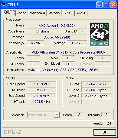
We weren't impressed with the power consumption of Brisbane at all in our first review; while it was lower than its 90nm counterpart, in many cases it wasn't all that much lower. Once again this is an issue of comparing a very mature 90nm process with AMD's first 65nm chips. You see, the voltages that Brisbane will be manufactured at range from 1.250V to 1.350V, with the coolest running, highest overclocking, least power consuming chips running at 1.250V and the worst examples running at 1.350V. Both of our Brisbane samples, the 5000+ and 4800+, ran at 1.350V. Note that our 90nm 5000+ ran at 1.300V, a lower voltage than the newer 65nm core. The fact that many 65nm parts aren't at much lower voltages yet is why the highest clocked Athlon 64 X2s are still 90nm CPUs, such as the 5600+ which runs at 2.8GHz.
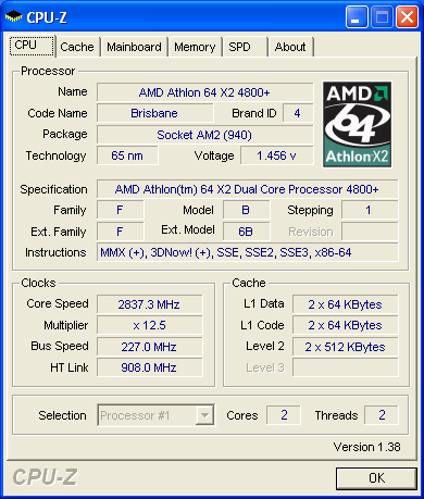
At some point in the future, AMD will hopefully be able to tune its manufacturing so that we will get lower voltage, lower wattage 65nm parts. This is also part of the reason why we encountered such dismal overclocking results with our 5000+. The 4800+ we tested fared no better, with our best overclock on stock cooling ending up at 2.837GHz (227 x 12.5) - not terrible for stock cooling, but not great either.
The impact of higher voltages on power consumption also applies to Intel as well. As you will see in our power comparison, in a number of cases our Core 2 Duo E6300 required even more power than the E6600 we tested last time. The reason being that our E6300 sample runs at a core voltage of 1.325V vs. 1.2625V for our E6600 sample. Just things to keep in mind as you look at the power results over the next few pages.
| CPU | Core Voltage of our Test Chip |
| AMD Athlon 64 X2 5000+ (90nm) | 1.3000V |
| AMD Athlon 64 X2 4600+ EE (90nm) | 1.2500V |
| AMD Athlon 64 X2 3800+ EE SFF (90nm) | 1.0750V |
| AMD Athlon 64 X2 5000+ EE (65nm) | 1.3500V |
| AMD Athlon 64 X2 4800+ EE (65nm) | 1.3500V |
| Intel Core 2 Duo E6600 (65nm) | 1.2625V |
| Intel Core 2 Duo E6400 (65nm) | 1.3125V |
| Intel Core 2 Duo E6300 (65nm) | 1.3250V |
Brisbane Performance Issues Demystified: Higher Latencies to Blame
As you'll remember from Part 1, for some reason, our 65nm Athlon 64 X2 5000+ performed slower than our 90nm part. We had contacted AMD before publication of the article but didn't receive a response until after we were well underway with Part 2. AMD's explanation for the reduced performance? Higher memory latencies.
We wanted to investigate exactly how much higher, thus we turned to CPU-Z's latency benchmark to give us a quick indication of how things had changed.
| CPU | CPU-Z Latency (8192KB, 128-byte) |
| AMD Athlon 64 X2 5000+ (65nm) | 122 cycles (46.92 ns) |
| AMD Athlon 64 X2 5000+ (90nm) | 121 cycles (46.54 ns) |
A single cycle increase in memory access latency, or 0.4ns, is a slight increase but not enough to cause the sort of performance deltas we saw in Quake 4 and Half Life 2, something else was amiss. Luckily it was another metric that CPU-Z's latency test reported that helped us understand the cause of the poor performance: L2 cache access latency.
| CPU | CPU-Z L2 Cache Latency | ScienceMark 2.0 L2 Cache Latency |
| AMD Athlon 64 X2 5000+ (65nm) | 20 cycles | 20 cycles |
| AMD Athlon 64 X2 5000+ (90nm) | 12 cycles | 12 cycles |
Updated - 1/5/07: Although AMD previously did not mention any issues with our findings, we were contacted today and informed that the latency information both ScienceMark and CPU-Z produced is incorrect. The Brisbane core's L2 latency should be 14 cycles, up from 12 cycles and not 20 cycles. This would help explain the relatively low impact on application performance that we've seen across the board. We are still waiting to hear back from AMD on a handful of other issues regarding Brisbane and will update you as soon as we have more information.
The original K8 core, in both 130nm and 90nm flavors, had a 12-cycle L2 cache. With Brisbane, as reported by both CPU-Z and ScienceMark, 65nm K8 now has a 20-cycle L2 cache. Generally speaking you move to a higher latency cache if you're planning on introducing a larger cache size, but a quick glance at AMD's roadmaps doesn't show anything larger than a 1MB L2 per core for the next year. The argument for higher clock speeds isn't valid either as the highest clock speed on AMD's roadmaps thus far is only 3.2GHz.
Luckily the performance impact of the higher latency L2 cache isn't noticeable in all applications, thanks to the K8's on-die memory controller, but make no mistake - the new core is slower. We couldn't figure out why AMD made the change and with most of our key AMD contacts on vacation due to the holidays, we still have no official response on the matter. Rest assured that if/when we learn more we will let you know.
Updated: AMD has given us the official confirmation that L2 cache latencies have increased, and that it purposefully did so in order to allow for the possibility of moving to larger cache sizes in future parts. AMD stressed that this wasn't a pre-announcement of larger cache parts to come, but rather a preparation should the need be there to move to a vastly larger L2. Thankfully the performance delta isn't huge, at least in the benchmarks that we saw, so AMD's decision isn't too painful - especially as it comes with the benefit of a cooler running core that draws less power; ideally we'd like the best of all worlds but we'll take what we can get. Note that none of AMD's current roadmaps show any larger L2 parts (other than the usual 2x1MB offerings), which tells us one of two things: either AMD has some larger L2 parts that it's planning on releasing or AMD is being completely honest with the public in saying that the larger L2 parts will only be released if necessary.
The Test
For each benchmark we measured performance as well as average power consumption during the course of the benchmark, finally reporting performance per watt as one divided by the other. Both Cool 'n Quiet and EIST were enabled on all processors.
| CPU: | Intel Core 2 Duo E6600 (2.40GHz/4MB) AMD Athlon 64 X2 5000+ (2.6GHz/512KBx2) AMD Athlon 64 X2 5000+ EE "Brisbane" AMD Athlon 64 X2 4800+ EE "Brisbane" AMD Athlon 64 X2 EE 4600+ (2.4GHz/512KBx2) AMD Athlon 64 X2 EE SFF 3800+ (2.0GHz/512KBx2) |
| Motherboard: | eVGA NVIDIA nForce 680i ASUS M2N32-SLI Deluxe |
| Chipset: | nForce 680i nForce 590 SLI |
| Chipset Drivers: | NVIDIA 9.53 NVIDIA 9.35 |
| Hard Disk: | Seagate 7200.9 300GB SATA |
| Memory: | Corsair XMS2 DDR2-800 4-4-4-12 (1GB x 2) |
| Video Card: | NVIDIA GeForce 8800 GTX |
| Video Drivers: | NVIDIA ForceWare 97.44 |
| Resolution: | 1600 x 1200 |
| OS: | Windows XP Professional SP2 |
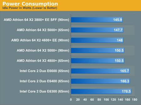
Idle Power Consumption
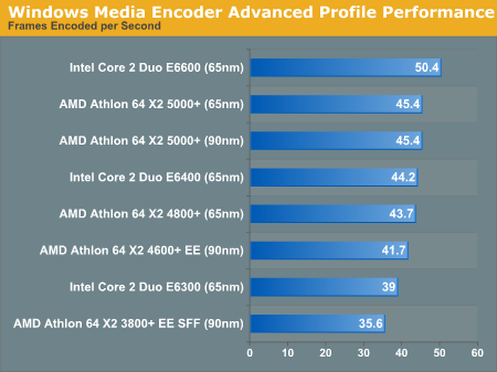
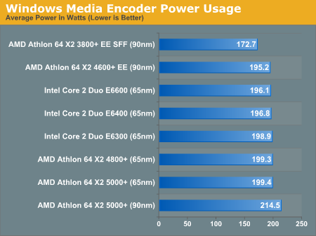
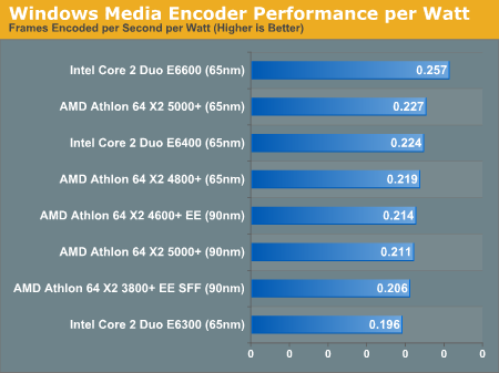
Media Encoding Performance & Power Consumption
The absolute performance crown under our WME test continues to belong to the E6600, followed by the X2 5000+, but after that it's a fairly close race between the contenders. The E6400 and X2 4800+ are basically equal in performance, with the 4600+ following closely. At the low end of the spectrum, the E6300 outperforms the X2 3800+ but albeit with much higher power consumption.
If we look at absolute power consumption, the X2 3800+ EE SFF can't be beat. Although it's outperformed by every other chip in the test, it consumes at least 20 fewer watts during the benchmark. Power consumption for the rest of the chips is basically equal, with the 90nm X2 5000+ sticking out as the only sore thumb.
Our E6300 sample's combination of high operating voltage and low performance relative to the competition results in it having the worst performance per watt out of the group. The X2 3800+ SFF comes in second to last in this metric due to its lower performance. Meanwhile, the E6600 places first, the 65nm X2 5000+ is in second place, closely followed by Intel's Core 2 Duo E6400 and the 65nm X2 4800+.
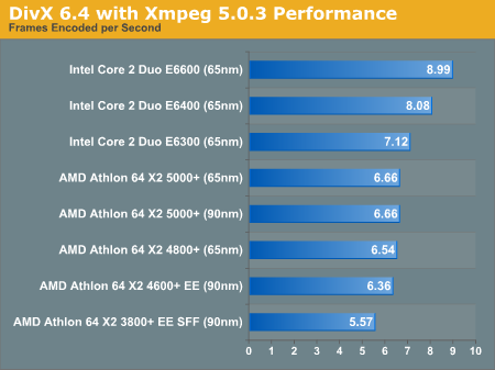
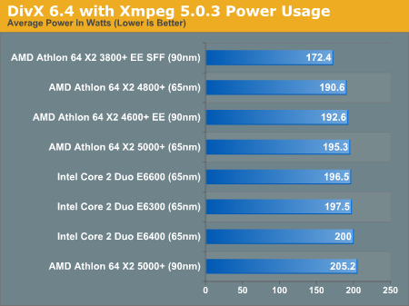
DivX performance favors Intel much more than our WME test, as the top three performance spots go to Intel. There's no performance difference between AMD's 90nm and 65nm chips in this test as both 5000+ CPUs are tied at 6.66 fps.
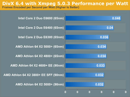
The absolute power advantage goes, once again, to the X2 3800+ EE SFF. Our 65nm 4800+ sample draws a bit less power than the 5000+ and even manages to draw less than the 90nm 4600+ EE. Unfortunately with no great power advantages and mid-range performance, the top three in the performance per watt category belong to Intel.
Media Encoding Performance & Power Consumption (Continued)
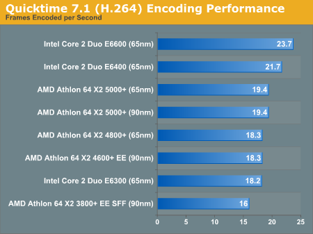
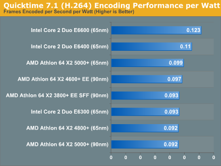
The standings don't change much in our QuickTime test, with Intel taking top honors. The 5000+ chips are tied for performance but the 65nm chip uses quite a bit less power. Performance per watt echoes the performance chart, but the 90nm 5000+ drops to the bottom, with everything lower than the 4600+ EE clustering close together.

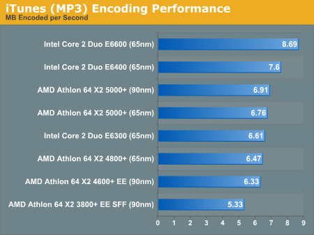
Our iTunes test is the first place where we see a small difference between AMD's 90nm and 65nm cores, in this case the older core has an advantage of just over 2%. The highest performer is clearly the E6600, followed by the E6400. The E6300's lower clock speed puts it in between the X2 5000+ and 4800+.
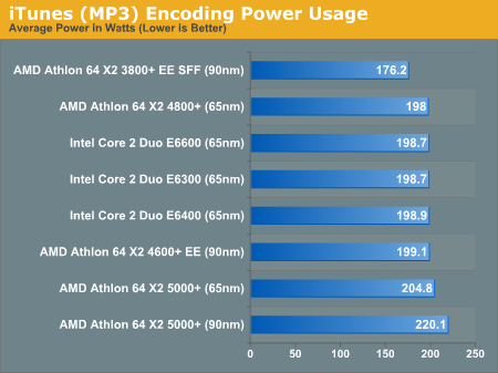
Power consumption is the same old story, with AMD's EE SFF chip drawing the least power while the 90nm X2 5000+ pulls the most. The rest of the contenders basically use about the same amount of power.
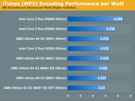
Looking at performance per watt, once again we have the E6600 and E6400 out on top, and the Brisbane cores tie with the E6300 in the middle of the pack.
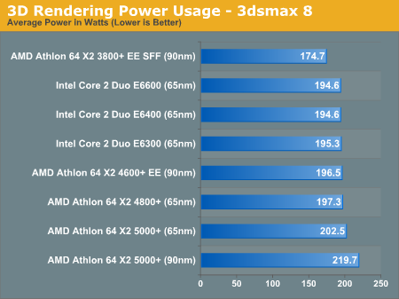
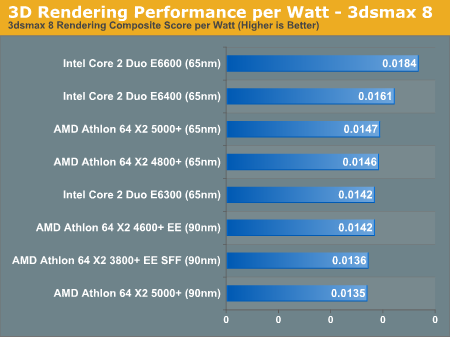
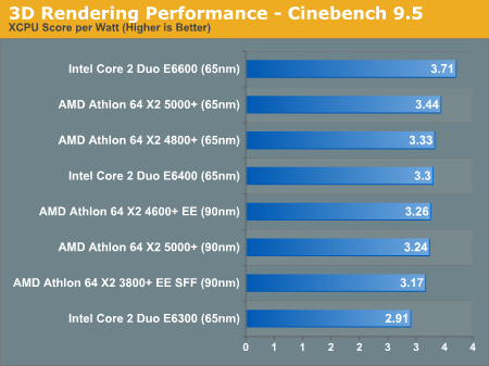
3D Rendering Performance & Power Usage
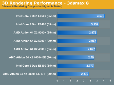
3D rendering performance under 3dsmax 8 continues to be a strong suit of Intel's, but the E6600's advantage is narrowed dramatically by the lower clock speed and smaller cache size of the E6400. Take price into account, and the E6400 is clearly the winner here. Once again, there's no real performance difference between the 90nm and 65nm AMD cores here, which is quite impressive given the significantly higher L2 access penalty with Brisbane.
Average power consumption under 3dsmax 8 is in line with what we've been seeing thus far, and taking both performance and power into account gives us similar results as well.
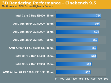
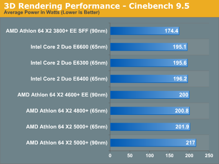
Performance under Cinebench is closer between AMD and Intel, which also impacts the performance per watt results. There's a slight performance difference between the Windsor (90nm) and Brisbane (65nm) cores, but nothing to write home about.
Gaming Performance & Power Usage
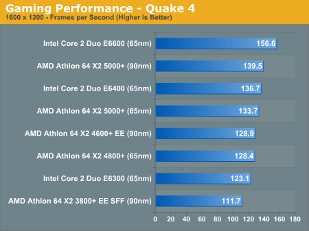
Quake 4 was the first application that really showed us the performance penalty you incur when moving to Brisbane, in this case the older core is about 4% faster. If you take into account that we're looking at performance at 1600 x 1200 with a GeForce 8800 GTX, in more GPU limited situations you're unlikely to notice the performance difference, but at more CPU limited situations the delta could likely grow even larger than 4%.
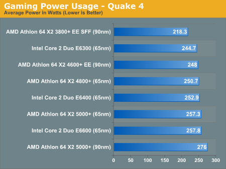
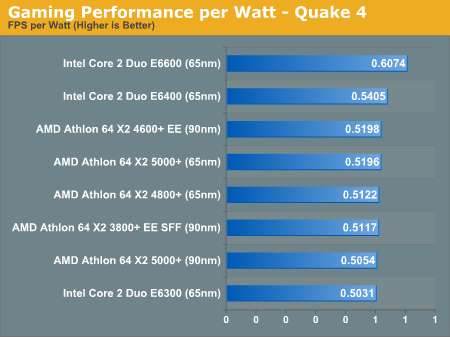
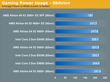
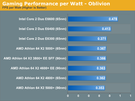
As the Core 2 processors are pushing much more data to the GPU than their competitors, average power consumption is generally much higher - it's the expense of greater performance in this case. The performance per watt charts take into account both factors and give you more of a breakdown of efficiency. Despite the decrease in performance, the reduction in power consumption gives the new Brisbane cores the efficiency advantage over most of their predecessors.
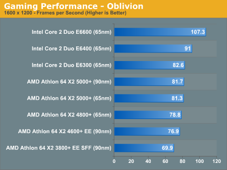
Oblivion didn't show a real impact in performance due to the slower Brisbane cores, but it clearly favors Intel's Core 2 architecture over AMD's.
Gaming Performance & Power Usage (Continued)
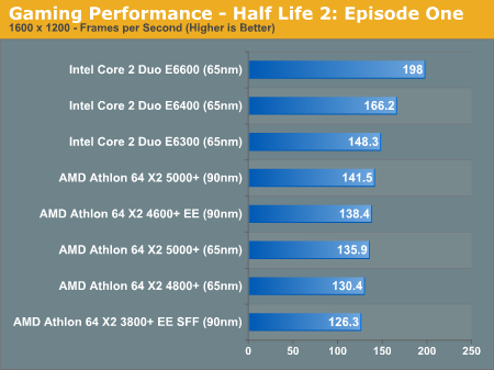
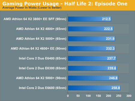
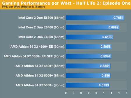
Half Life 2: Episode One agreed with Quake 4, showing a 4% decrease in performance when going to the new 65nm 5000+. It also clearly favors the Core 2 architecture, with even the E6300 placing ahead of the 5000+ in the performance chart.
Final Words
Now that the pieces are falling into place we are able to understand a bit more about the implications of AMD's move to 65nm. It's clear that these first 65nm chips, while lower power than their 90nm counterparts, aren't very good even by AMD's standards. Already weighing in at the high end of the voltage spectrum, we hope to see more overclockable, lower power offerings once AMD's 65nm ramp really starts up. It's a constantly evolving process and if this is the worst we will see, it's not terrible; AMD can only go up from here, but it does mean that you shouldn't hold your breath waiting for the right 65nm AMD to come along.
Performance and efficiency are still both Intel's fortes thanks to its Core 2 lineup, and honestly the only reason to consider Brisbane is if you currently have a Socket-AM2 motherboard. It is worth mentioning that AMD still has the lowest overall power use with its Athlon 64 X2 EE SFF processor, but in terms of performance per watt efficiency it's not all that great. We would really like to see an EE SFF successor built on AMD's 65nm process, but we have a feeling it will be a little while before we are graced with such a delicate creature.
The step back in performance with Brisbane is truly puzzling; while none of our individual application benchmarks showed a tremendous loss in performance, it's a very unusual move for AMD. The last thing AMD needs to do is take away performance, and based on its current roadmaps the higher latency L2 cache makes no sense at all. Either AMD has some larger L2 cache variants in the works that we're not aware of, or AMD's cache didn't take very kindly to the 65nm shrink. As soon as we get the official word as to why L2 access latencies jumped 66% with Brisbane we'll be sure to report it; until then we can only wonder.
We long for the good old days, when a die shrink meant ridiculously overclockable processors, back before a die shrink was coupled with a sneaky decrease in performance. While Brisbane is far from a Prescott, it's not exactly what we were hoping for from AMD's first 65nm Athlon 64 X2. Hopefully they can work out some of the process' kinks in time for the K8L launch.


