Original Link: https://www.anandtech.com/show/2198
EVGA 680i LT SLI: NVIDIA's 680i Cost Reduced
by Gary Key on March 28, 2007 4:00 AM EST- Posted in
- CPUs
Since our first look at the 680i SLI chipset back in November we have been impressed with its performance and overall features. What was even more impressive was the fact that the chipset debuted on a motherboard that was designed by NVIDIA and built for NVIDIA's launch partners. This launch basically followed the path of the successful AM2 590SLI introduction except this time NVIDIA introduced and marketed the only board available with the 680i SLI chipset through a select number of partners. Although the 680i SLI motherboard was a reference design, it catered to the computer enthusiasts with a long list of features and a BIOS specifically aimed at the overclocking community.
It was several weeks before a motherboard manufacturer would offer a competing 680i solution. ASUS was the first non-reference board partner to offer competition to NVIDIA's reference design and it would take a few months before the likes of abit and Gigabyte were able to respond with their internal designs. We are still waiting on DFI's version to come to market and other motherboard manufacturers such as ECS and Biostar decided it was in their best interest to offer the reference board design that is built by Foxconn. The majority of NVIDIA's motherboard reference partners are actually heavily involved in the distribution of their graphics solutions with EVGA being the focal point of NVIDIA's reference program at this time.
The 680i SLI chipset has had a bumpy introduction with numerous issues being discovered and eventually fixed through a series of BIOS releases or new board revisions. The latest incarnation of the 680i SLI reference design from EVGA has solved our last remaining issues that concerned quad core overclocking performance. The non-reference partners have solid designs that have been hampered by immature BIOS releases but even those issues are starting to be resolved with the latest BIOS updates. While the 680i SLI based motherboards are finally on the right track from a performance and compatibility viewpoint, the pricing on these boards have been embarrassingly expensive to date. We have seen prices ranging from a low of $199 (EVGA 680i SLI board with rebate) to just over $400 for the ASUS Striker Extreme. On average, the majority of the 680i SLI boards sell in the $250 and up range.
With the 650i SLI boards just coming to market in volume and the 650i Ultra boards still not available, NVIDIA has had a difficult time in the Intel market from a competitive cost position. NVIDIA is starting to address that issue and is lowering the cost of entry into the mid to upper performance market with its new 680i LT SLI chipset. Like the 680i SLI chipset launch, this junior member of the 680i family will be available on a reference board design through a select number of partners as of this week. Once again, EVGA is one of the first partners to market with their 680i LT SLI motherboard priced at a more reasonable $199 (currently $174.99 with rebate). This is $50 less than the standard $249 MSRP for the 680i SLI reference boards but only $10 to $20 less than current street prices with rebates. This small difference in pricing could come back to haunt NVIDIA in the end, but we will have to see what street prices are before coming to any final conclusion.
Of course, before presenting performance results and discussing the complexities of this new reference design we need to first explain the differences between the 680i SLI and 680i LT SLI chipsets. We basically believe the 680i LT SLI SPP is a renamed 680i SLI SPP that has been feature reduced or more than likely neutered by the BIOS. The LT SPP carries the C55-P-N-A2 part number designation with its big brother being labeled with a C55-SLIX16N-A2 moniker. The real differences in the chipsets are in their choice of MCPs with the 680i LT utilizing the nForce 570 SLI MCP and the 680i SLI sporting the nForce 590 SLI MCP. It is always interesting to see how many times a recent NVIDIA MCP can be utilized in a different design or paired up with an ever increasing amount of SPP choices. We have to hand it to NVIDIA for having the ability to mix and match chipsets at will to create to new product line, but the constant renaming of the same chipsets has become tiresome and at times confusing.
With the chipset designations out of the way, let's see what the real differences are at this time. Both chipsets officially support front-side bus speeds up to 1333MHz so support for the upcoming Intel processors are guaranteed as is a certain amount of overclocking headroom. Both chipsets advertise "best-in-class" overclocking capability with the 680i SLI officially being termed "best" in this regard by NVIDIA. We think they are both equal but due to BIOS limitations we will probably never find out.
The 680i SLI offers full support for Enhanced Performance Profile (SLI-Ready) memory at speeds up to 1200MHz with the LT version only offering official 800MHz support. However, this only means you will have to tweak the memory speed and timings yourself in the BIOS, something most enthusiasts do anyway. We had no issue running our LT equipped board memory speeds up to 1275MHz so this feature deduction is not a real issue, although we wonder why they even offered limited support. Either do it all the way or don't do it all in our opinion.
Also missing in action is the Link Boost functionality that allows for an automatic 25% increase in the speed of the HyperTransport links that connect the SPP and MCP chipsets when utilized with an approved GeForce graphics solution. Although the performance improvements in benchmarks have been minimal to date, we have seen some minor increases in certain benchmarks with the 8800GTX cards. However, the GPU Ex option is available as is the QuickSync technology that improves memory performance when the memory is operating in sync mode. Once again, we have seen minimal performance differences in actual applications but every little bit helps.
The real differences between the chipsets are the missing features on the LT chipset. These include the loss of two USB ports (10 down to 8) and a Gigabit Ethernet port. The DualNet teaming feature is no longer available but will probably not be missed by the vast majority of users, nor will the loss of the second Ethernet port. However, the loss of two USB ports could cause issues with users who have several USB based peripherals.
One of the last options to go is the third physical PCI Express x16 slot that operated at x8 speeds electrically. While the primary purpose for this slot centered on adding a third graphics card for physics acceleration that is still not available, it will be missed by users who had x4 or x8 devices such as PCI Express based RAID controller cards. The remaining differences between the boards is the lack of a passive cooling solution, LED post code display, onboard power and reset buttons, and speaker. Last, but by no means least, is an option reduced BIOS that is designed to offer just enough options to overclock the board to a certain degree, but it is missing just enough options to frustrate most users who will be purchasing this board based on its performance capabilities.
This leads us into today's performance review of the EVGA 680i LT SLI. In our article today we will briefly go over the board layout and features, provide a few important performance results, and discuss our findings with the board. We will provide further in-depth performance results of this product in a later article. With that said, let's take a quick look at this interesting board and see if it lives up to its hype.
Features and Specifications
| EVGA 680i LT SLI | |
| Market Segment: | High-End Performance - $199 |
| CPU Interface: | Socket T (Socket 775) |
| CPU Support: | LGA775-based Pentium 4, Celeron D, Pentium D, Pentium EE, Core 2 Duo, Core 2 Extreme |
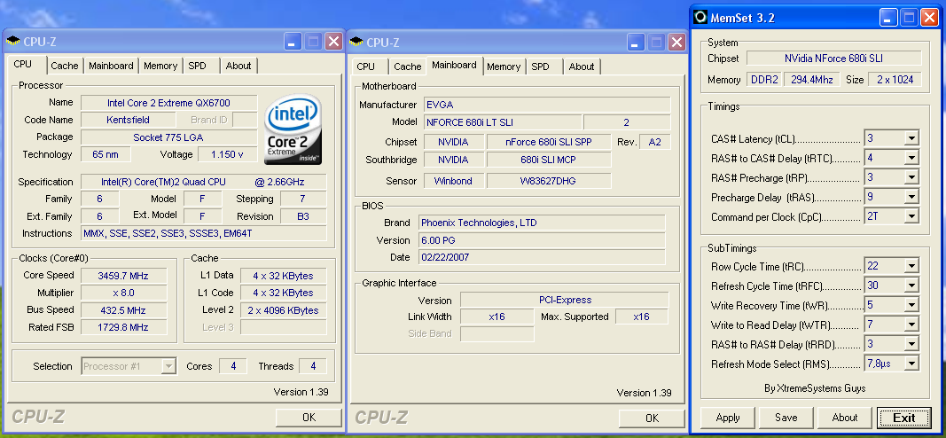
| Chipset: | NVIDIA 680i LT SPP (C55 P-N-A2) + 680i LT MCP (570 SLI MCP) |
| Bus Speeds: | Auto, 400 to 2500 QDR (100~625) in 1MHz increments |
| Memory Ratios: | Auto, Sync., 1:1, 5:4, 3:2 |
| Memory Speed: | 400MHz~1400MHz in various increments |
| PCIe 1&2 Speeds: | 100MHz~200MHz in 1MHz Increments |
| HT Multipliers: | 1x, 2x, 3x, 4x, 5x |
| Core Voltage: | Auto, 0.80000V to 1.60000 in 0.00625V increments |
| FSB Options: | Auto, Linked, Unlinked |
| CPU Clock Multiplier: | Auto, 6x-11x in 1X increments - Core 2 Duo, downwards unlocked, Core 2 Extreme 6x-60X |
| DRAM Voltage: | Auto, 1.80V to 2.50 in .10V increments |
| DRAM Timing Control: | Optimal, Expert - 10 DRAM Timing Options |
| NB Voltage: | Auto, 1.2V, 1.3V, 1.4V |
| FSB Voltage: | Auto, 1.2V, 1.3V, 1.4V |
| Memory Slots: | Four 240-pin DDR2 DIMM Slots Dual-Channel Configuration, DDR2-400, 533, 667, 800 Regular Unbuffered Memory to 8GB Total |
| Expansion Slots: | 2 - PCIe X16 (2-x16 electrical for SLI or Multi-GPU) 2 - PCIe x1 2 - PCI Slot 2.2 |
| Onboard SATA/RAID: | 6 SATA 3Gbps Ports - 570 SLI MCP (RAID 0,1, 0+1, 5, JBOD) |
| Onboard IDE: | 1 ATA133/100/66 Port (2 drives) - 570 SLI MCP |
| Onboard USB 2.0/IEEE-1394: | 8 USB 2.0 Ports - 4 I/O Panel - 4 via Headers 2 Firewire 400 Ports by TI TSB43AB22A - 1 I/O Panel, 1 via Header |
| Onboard LAN: | NVIDIA Gigabit Ethernet - PCIe - Marvell 88E1116 PHY - 1 port via 570 SLI MCP |
| Onboard Audio: | Realtek ALC885 - 8-channel HD audio codec |
| Power Connectors: | ATX 24-pin, 8-pin EATX 12V, 4-pin 12V Molex |
| I/O Panel: | 1 x PS/2 Keyboard 1 x PS/2 Mouse 1 x S/PDIF Optical - Out 1 x IEEE 1394a 1 x Audio Panel 1 x RJ45 4 x USB 2.0/1.1 |
| BIOS Revision: | Award 721N0P01 |
| Board Revision: | v1.0 |
The NVIDIA reference BIOS offers a moderate level of options available for tweaking the board with emphasis placed on the available memory settings. We found in memory testing that switching to manual settings and changing the tCAS, tRCD, tRP, and tRAS was required to ensure optimum performance as our performance results will show shortly.
Compared to the standard 680i BIOS the ability to control the HT and MCP voltages is not available, and FSB and SPP voltages are limited to 1.4V. The inability to change FSB VTT or GTL Ref voltage settings limited our overclocking results to some degree, but more importantly the lack of higher FSB/SPP voltages basically capped our board sample at 500FSB.
One other issue we have with the "Lite" BIOS is that memory voltages are limited to .10V increments meaning that in several cases we could not fine tune our ProMOS or Elpida modules for optimum performance. While we understand NVIDIA's desire not to have this board compete directly with the 680i boards, some of the cuts made are generally frustrating for extracting the best performance out of this board.
 |
| Click to enlarge |
EVGA utilizes the standard NVIDIA nTune system utility but in yet another weird BIOS decision the ability to control voltages and fan speeds is non-existent. This ensures that any significant changes required for overclocking the board will have to be done via the BIOS. This is an operation that most people normally do anyway when overclocking, but one of the strengths of NVIDIA's reference boards has been their tight integration with nTune. The inability to control even the CPU fan is inexcusable considering this is a designed by NVIDIA board. Hopefully, the next BIOS release will address these two issues, and we certainly would like see additional voltage controls and automatic fan speed control for the other chassis fan headers. Of course, NVIDIA could really surprise us and offer fan control over the active chipset coolers.
Board Layout and Design
 |
| Click to enlarge |
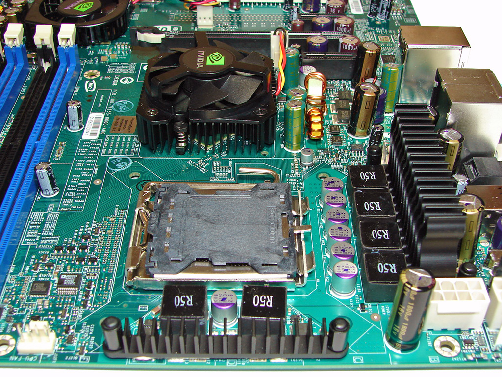
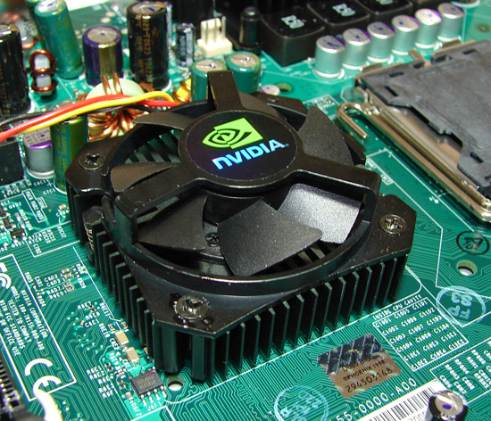
The board layout that NVIDIA devised for the 680i LT chipset is quite good but we would have preferred a black PCB design instead of the pedestrian green. The board easily installed into our Cooler Master CM Stacker 830 case while cable management was good for the optical and hard drives. The board features an excellent six-phase power design and a mixture of conductive polymer aluminum solid capacitors and high-quality aluminum electrolytic capacitors. There are four fan headers (one 4-pin, three 3-pin) located in easy to reach positions on the board but only the CPU fan offers automatic fan control capabilities within the BIOS. Both the SPP and MCP are actively cooled with fans that tended to have a noticeable whine on power-up and remained at 100% speed throughout testing as fan speed cannot be controlled.
Considering other boards in the price range have passive cooling solutions we have to question NVIDIA's decision on using an active cooling solution. We know this is one of the areas targeted for cost reduction but most people will find the noise obtrusive at times, and we are also concerned about the life expectancy of the fans. We do not mind active cooling solutions on chipsets that run hot or on a board designed with overclocking in mind. However, one of the main design objectives with this board was not to encroach upon the 680i boards in overclocking capabilities so this decision is slightly confusing to us.
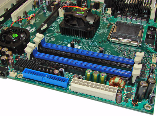
The memory slots are color coded correctly for dual channel operation. The 24-pin ATX power connector is conveniently located with the blue IDE connector on the edge of the board. We would have flipped the IDE connector to a right angle design in order to have opened up a little additional room for the four black SATA ports and 4-pin Molex connector. Unfortunately, one of the worst design decisions on this board was placing the chassis connector panel in between the Molex connector and the fourth DIMM slot.
The two primary black SATA ports and the floppy drive connector are located on the edge of the board. We found the positioning of the SATA ports to be very good when utilizing the PCI or second PCI-E x16 physical slot. The MCP is actively cooled and remained fairly warm to the touch throughout testing, although additional cooling was not needed when overclocking. The fan has a low profile and we did not have any issue using our 8800GTX, but again the area around it tended to get hot after stress testing.
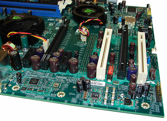
The board comes with two PCI Express x16 connectors, two PCI Express x1, and two PCI connectors. The layout of this design offers a good but not spectacular dual x16 connector design. The second PCI Express x1 slot will be physically unavailable as will the second PCI connector if you utilize a double slot card in either x16 slots. We would also have switched the first PCI and second PCI Express x16 connector in order to give the second video card additional space, as our secondary 8800GTX tended to act like a vacuum cleaner for the bottom of our case. It would have been nice if the second PCI Express x1 connector had been moved to the vacant spot where the missing third x16 slot would have been located. This would have meant that both PCI Express x1 slots would have been open even with dual-slot SLI.
 |
| Click to enlarge |
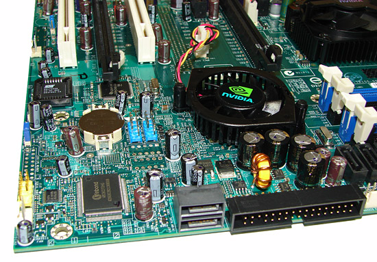
Getting back to the CPU socket area, we find an excellent amount of room for alternative cooling solutions. We utilized the stock heatsink/fan in our normal testing but also verified a few larger Socket-775 air cooling solutions would fit in this area during our overclocking tests. The 680i LT SPP chipset is actively cooled with a mid-rise heatsink/fan unit that did not interfere with any installed peripherals but was loud in our opinion. The VRM components are passively cooled and the 8-pin ATX power connector is located out of the way.
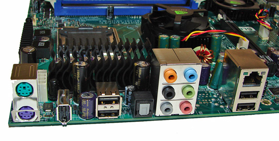
The rear panel contains the standard PS/2 mouse and keyboard ports, LAN port, and four USB 2.0 ports. The LAN port has two LED indicators representing Activity and Speed of the connection through the Marvell Gigabit PCI-E PHY. The audio panel consists of six ports that can be configured for 2, 4, 6, and 8-channel audio along with an S/PDIF optical out port. The I/O panel also features an IEEE 1394a port.
The audio subsystem is based on the Realtek ALC885 and offers 8-channel output. Realtek has had troubles recently with EAX 2.0 support but we did notice a slight improvement in the 1.61 driver set with several games, although Battlefield 2 continues to present problems for Realtek. We continue to feel that the ADI 1988B HD audio codec on the upper end ASUS boards or the Creative X-Fi chipset utilized on the new MSI 680i offer significantly better EAX audio quality in games than the Realtek HD codecs.
Overall, the feature set on this board is good but other boards in this price range offer additional USB and network ports along with passive cooling designs.
Overclocking - E6300
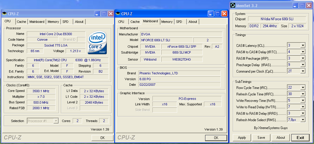
| EVGA 680i LT SLI Dual Core Overclocking Testbed |
|
| Processor: | Intel Core 2 Duo E6300 Dual Core, 1.86GHz, 2MB Unified Cache 1066FSB, 7x Multiplier |
| CPU Voltage: | 1.4500V (default 1.3250V) |
| NB Voltage: | 1.40V |
| FSB Voltage: | 1.40V |
| Cooling: | Tuniq 120 Air Cooling |
| Power Supply: | OCZ ProXStream 1000W |
| Memory: | OCZ Flex XLC PC2-6400 (2x1GB) (ProMOS Memory Chips) |
| Video Cards: | 1 x MSI 8800GTX |
| Hard Drive: | Western Digital 150GB 10,000RPM SATA 16MB Buffer |
| Case: | Cooler Master CM Stacker 830 |
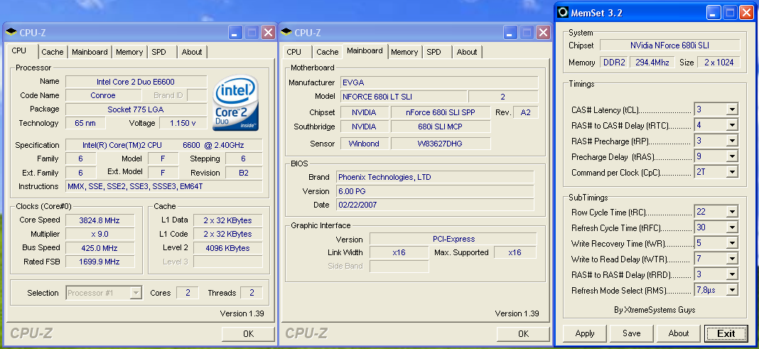
| Maximum OC: | 500x7 (3-4-3-9 2T, 800MHz, 2.20V), CPU 1.4500V 3500MHz (+88% FSB/CPU) |
| . | |
 |
| Click to enlarge |
We were easily able to reach a final benchmark stable setting of 7x500 FSB resulting in a clock speed of 3500MHz. We were able to run our OCZ Flex PC2-9200 and Corsair PC2-8888 at the reported timings with a 1T Command Rate enabled with 2.30V. However, when overclocking we had to run our standard OCZ Flex PC2-6400 at 2T command rates due to the next voltage step being 2.30V, a setting that is not recommended for the ProMOS chips (2.250V is our recommended limit for 24/7 operation). Vdroop was very acceptable on this board during overclocking with an average drop of .02 ~.03V during load testing with our E6300.
Testing with our new OCZ Flex PC2-6400 CAS3 (standard memory installed) and G.Skill F2-6400CL4D-2GBHK modules based on the ProMOS IC chips resulted in great success on this board. The OCZ Flex PC2-6400 was able to run at DDR2-800 speeds with timings at 3-4-3-9 2T at 2.15V and the G.Skill F2-6400CL4D at 4-3-3-8 2T at 2.15V on our other NVIDIA boards but we had to use the 2.20V setting. The remaining memory timings are set to Auto as is standard in our testing and manually setting these timings resulted in minimal performance gains. We did notice in 4GB testing that we had to change our OCZ Flex PC2-6400 CAS3 memory timings to 3-4-4-12 2T at 2.20V for stable 24/7 operation in a variety of applications.
Overclocking - E6600
| EVGA 680i LT SLI Dual Core Overclocking Testbed |
|
| Processor: | Intel Core 2 Duo E6600 Dual Core, 2.4GHz, 4MB Unified Cache 1066FSB, 9x Multiplier |
| CPU Voltage: | 1.4750V / 1.4500 (default 1.3250V) |
| NB Voltage: | 1.40V |
| FSB Voltage: | 1.40V |
| Cooling: | Tuniq 120 Air Cooling |
| Power Supply: | OCZ ProXStream 1000W |
| Memory: | OCZ Flex XLC PC2-6400 (2x1GB) (ProMOS Memory Chips) |
| Video Cards: | 1 x MSI 8800GTX |
| Hard Drive: | Western Digital 150GB 10,000RPM SATA 16MB Buffer |
| Case: | Cooler Master CM Stacker 830 |
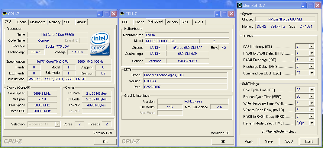
| Maximum CPU OC: | 425x9 (3-4-3-9 2T, 799MHz, 2.20V), CPU 1.4750V 3825MHz (+59%) |
| Maximum FSB OC: | 500x7 (3-4-3-9 2T, 800MHz, 2.20V), CPU 1.4500V 3500MHz (+88% FSB) |
| . | |
 |
| Click to enlarge |
After trying numerous settings and voltages we finally found a benchmark stable setting of 9x425 FSB resulting in a clock speed of 3825MHz. We did find the typical FSB hole around 416FSB that continued until 422FSB. We were able to post and complete benchmark testing at 432FSB but could not pass dual Prime95 at that setting. Vdroop was acceptable during overclocking with an average drop of .03 ~.04V during load testing with our E6600. We generally found that without decent airflow around the CPU and memory locations that our maximum FSB was near 410 MHz with this configuration.
 |
| Click to enlarge |
We dropped the multiplier on our E6600 to seven and were able to reach 500 FSB. We entered XP at 7x518 but the board was not stable due to a lack of higher FSB/SPP/MCP voltages. At first we thought the board was locked at 500FSB but once again we found FSB holes but this time they ranged from 502 to 516. We jokingly started to refer to this board as Swiss cheese during testing as everywhere we turned there was another FSB hole. If NVIDIA had offered VTT and GTL Ref Voltage options in the BIOS we are sure several of our holes could have been solved but we were still able to work around most of them.
In our overclock testing we were able to extract an 1133MHz memory speed at 5-5-5-15 2T timings with our OCZ Flex PC2-6400. This is the highest speed we have reached with this memory and at synced speeds we were able to reach DDR2-850 with timings at 3-4-4-9 2T on 2.20V. We dropped in our OCZ Flex PC2-9200 and Corsair PC2-9136 modules with both being able to reach DDR2-1275 with 5-5-4-12 2T timings at 2.30V. Memory performance and stability was excellent once the board was dialed in.
Overclocking - QX6700
| EVGA 680i LT SLI Quad Core Overclocking Testbed |
|
| Processor: | Intel Core 2 Extreme QX6700 Quad Core, 2.66GHz, 8MB Unified Cache 1066FSB, 10x Multiplier |
| CPU Voltage: | 1.4500V (default 1.3500V) |
| NB Voltage: | 1.40V |
| FSB Voltage: | 1.40V |
| Cooling: | Tuniq 120 Air Cooling |
| Power Supply: | OCZ ProXStream 1000W |
| Memory: | OCZ Flex XLC PC2-6400 (2x1GB) (ProMOS Memory Chips) |
| Video Cards: | 1 x MSI 8800GTX |
| Hard Drive: | Western Digital 150GB 10,000RPM SATA 16MB Buffer |
| Case: | Cooler Master CM Stacker 830 |
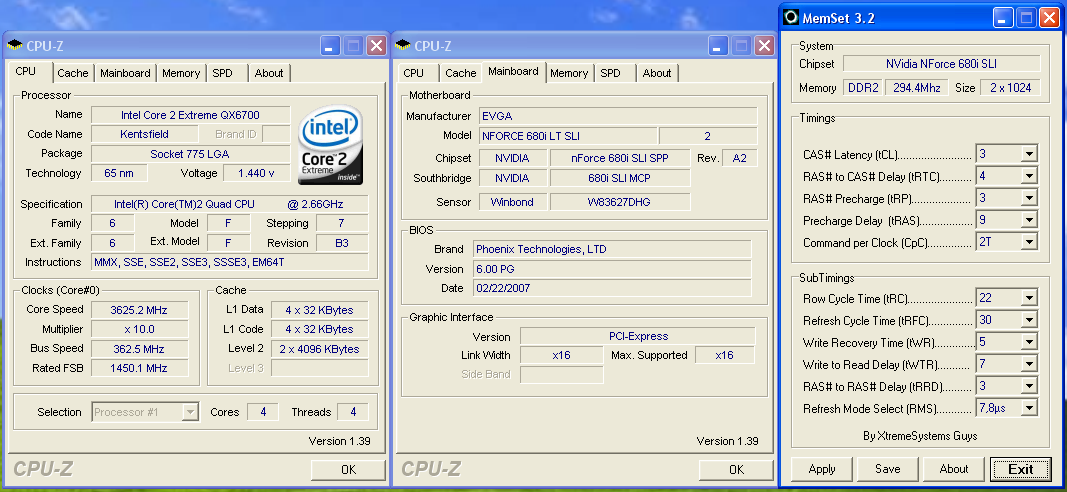
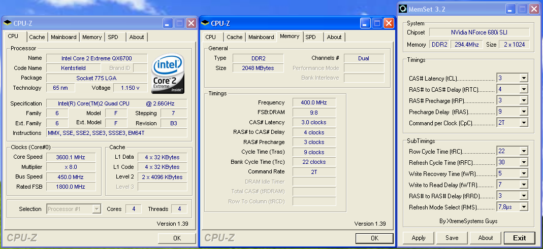
| Maximum OC: | 362x10 (3-4-3-9 2T, 797MHz, 2.20V), CPU 1.4500V 3625MHz (+36%) |
| Maximum FSB OC: | 432x8 (3-4-3-9 2T, 798MHz, 2.20V), CPU 1.4500V 3460MHz (+62% FSB) |
| . | |
 |
| Click to enlarge |
Needless to say, quad core overclocking on the 680i platforms has been a huge disappointment until recently. There is a new hardware revision of the EVGA 680i board and the latest BIOS on the ASUS Striker now allows 400+ FSB operation. Our board reached a final 362FSB at the stock multiplier and this was a setting that we found to be very stable during testing. We were able to POST and enter XP at 368FSB but could not complete our benchmark testing. Once again, the lack of voltage options hindered our results but they are still very good.
 |
| Click to enlarge |
 |
| Click to enlarge |
We dropped the multiplier on our QX6700 and were able to hit 8x450. The board completed the majority of our benchmarks at this setting but could not pass quad Prime95 or our four application multitasking test without the number three core waving the white flag. We finally reached a benchmark stable setting of 432FSB and probably could have gone higher but we had one of the dreaded FSB holes in the 440FSB range.
The one problem noted during testing is that we had to set our processor voltage to 1.4750V in order to maintain system stability. Our processor normally will run in the 3600MHz range at 1.4125V, and this was the highest voltage we have required on a board to reach this range. The reason for this is that Vdroop is terrible on this board with the quad core processor. We would see drops as high as .07V under load testing with the average drop being around .04V during game testing. The board also liked to "sing" to us while overclocked with the quad core installed. It was the one noise emitting from our case that we found to be louder than the chipset fans.
While we sound a bit pessimistic, this board did deliver results beyond our expectations in quad core testing. We just feel like a couple of the "corner cutting" activities inside the BIOS limited us once again from reaching the board's true capabilities.
Test Setup
| Standard Test Bed Performance Test Configuration |
|
| Processor: | Intel Core 2 Duo E6600 (2.4GHz, 4MB Unified Cache) |
| RAM: | OCZ Flex XLC PC2-6400 (2x1GB) 2.20V, 3-4-3-9 (1T where applicable) (ProMOS Memory Chips) |
| Hard Drive: | Western Digital 150GB 10,000RPM SATA 16MB Buffer |
| System Platform Drivers: | Intel - 8.1.1.1010 NVIDIA - 9.35, 8.43 ATI - 6.10 |
| Video Cards: | 1 x MSI 8800GTX |
| Video Drivers: | NVIDIA 97.92 |
| CPU Cooling: | Tuniq 120 |
| Power Supply: | OCZ ProXStream 1000W |
| Optical Drive: | Plextor PX-760A |
| Case: | Cooler Master CM Stacker 830 |
| Motherboards: | ASUS Striker Extreme (NVIDIA 680i) - BIOS 1002 ASUS P5N-E SLI (NVIDIA 650i) - BIOS 0401 ASUS P5B-E (Intel P965) - BIOS 0402 DFI LANParty UT ICFX3200-T2R/G (AMD RD600) - BIOS 12/22 EVGA 680i LT SLI (680i LT) - BIOS Award 721N0P01 GIGABYTE GA-N680SLI-DQ6 - BIOS F4B Intel D975XBX2 (Intel 975X) - BIOS 2333 MSI P6N SLI Platinum (nForce 650i) - BIOS 1.22 |
| Operating System: | Windows XP Professional SP2 |
| . | |
A 2GB memory configuration is standard in our XP test beds as most enthusiasts are currently purchasing this amount of RAM. Our choice of mid-range OCZ Flex XLC PC-6400 memory represents an excellent balance of price and performance that offers a very wide range of memory settings during our stock and overclocked test runs. We also utilized our Corsair XMS2 Dominator (Twin2x2048-9136C5D) memory on this board to verify DDR2-1066 to DDR2-1200 compatibility with another memory type.
We are currently completing testing of several other memory modules ranging from Transcend, TwinMOS, and WINTEC DDR2-800 down to A-DATA DDR2-533 for compatibility and performance benchmarks in our roundup article. Our memory timings are set based upon determining the best memory bandwidth via MemTest86 and test application results for each board. We only optimize the four main memory settings with sub-timings remaining at Auto settings.
We are utilizing the MSI 8800GTX video card to ensure our 1280x1024 resolutions are not completely GPU bound for our motherboard test results. We did find in testing that applying a 4xAA/8xAF setting in most of today's latest games created a situation where the performance of the system at our standard resolution did not really change. Our video tests are run at 1280x1024 resolutions for this article at High Quality settings. We also tested at 1600x1200 and 1920x1200 4xAA/8xAF for our NVIDIA SLI results that will be presented in our next article.
All of our tests are run in an enclosed case with a dual optical/hard drive setup to reflect a moderately loaded system platform. Windows XP SP2 is fully updated and we load a clean drive image for each system to ensure driver conflicts are kept to a minimum. We were able to run our memory test modules at 3-4-3-9 1T for our benchmark results and will be updating the results of our other boards with 1T operation shortly.
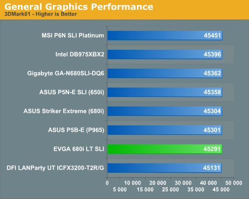
Synthetic Graphics Performance
The 3DMark series of benchmarks developed and provided by Futuremark are among the most widely used tools for benchmark reporting and comparisons. Although the benchmarks are very useful for providing apples-to-apples comparisons across a broad array of GPU and CPU configurations they are not a substitute for actual application and gaming benchmarks. In this sense we consider the 3DMark benchmarks to be purely synthetic in nature but still very valuable for providing consistent measurements of performance.
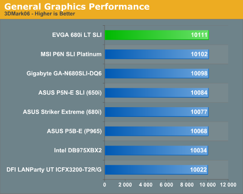
In our 3DMark06 test, each platform score is basically the same although we see the DFI RD600 based motherboard trailing slightly which we attribute to the slightly lower memory and video performance results in our latest BIOS release. Our EVGA board tops the chart and offers the best video performance of our test boards in this benchmark.
In the more memory and CPU sensitive 3DMark01 benchmark we see our EVGA 680i LT board trailing all boards but the RD600, although boards performed slightly better than the other 680i or 650i solutions in our Sandra benchmarks. Given the tight clustering of the scores, however, it is difficult to truly call any of the test candidates "faster" in these particular benchmarks.
General System Performance
The PCMark05 benchmark developed and provided by Futuremark was designed for determining overall system performance for the typical home computing user. This tool provides both system and component level benchmarking results utilizing subsets of real world applications or programs. This benchmark is useful for providing comparative results across a broad array of graphics, CPU, hard disk, and memory configurations along with multithreading results. We consider the PCMark benchmark to be both synthetic and real world in nature and again provided for consistency in our benchmark results.
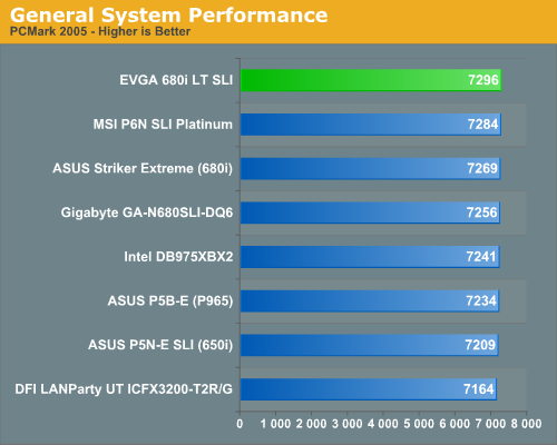
The EVGA 680i LT board tops our charts in this very competitive benchmark and we are starting to see a pattern emerge with the latest NVIDIA board release performing slightly better than our previous champ, the MSI P6N SLI Platinum. The 650i and 680i chipsets scored very well on the single task disk benchmarks with the 680i performing slightly better in the graphics subsystem tests where they led the field. However, our 975X and P965 chipset boards won the multi-tasking tests while the RD600 offered middle of the road performance in most of the tests.
Heavy Multitasking
We devised a script that would compress our standard test folder consisting of 444 files, ten subfolders, and 602MB worth of data, convert a 137MB High Definition QuickTime movie clip to a 37MB MPEG-4 format, play back the first two chapters of Office Space with PowerDVD, and run our AVG anti-virus program in the background. We stop the script when the file compression and video conversion are complete. This is a very taxing script for the CPU, memory, and storage subsystems. We also found it to be a good indicator of system stability during our overclocking testing.
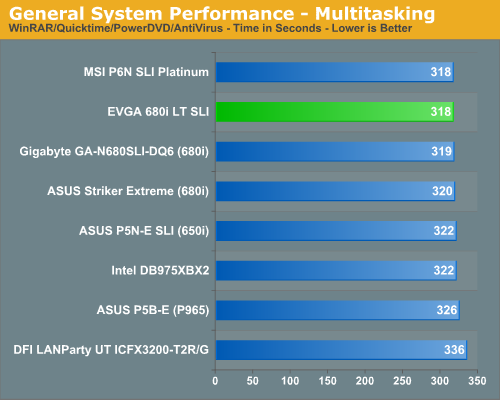
The performance difference basically mirrors our PCMark 2005 multithreaded test results with the MSI and EVGA boards finishing first due to great disk performance, although the Intel boards consistently completed the QuickTime conversion first. The DFI RD600 board scored last although it generated the best overall video playback results.
Media Encoding Performance
Our first encoding test is quite easy: we take our original Office Space DVD and use AnyDVD Ripper to copy the full DVD to the hard drive without compression, thus providing an almost exact duplicate of the DVD. We then fire up Nero Recode 2, select our Office Space copy on the hard drive, and perform a shrink operation to allow the entire movie along with extras to fit on a single 4.5GB DVD disc. We leave all options on their defaults except we turn off the advanced analysis option. The scores reported include the full encoding process and are in seconds, with lower numbers indicating better performance.
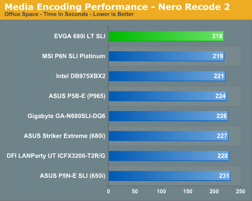
We continue to see a strong performance from the EVGA 680i LT SLI in our application tests with it once again finishing ever so slightly in front of the MSI board. In previous testing our ASUS 650i and 680i boards were almost two minutes slower in this test as we consistently found the performance of the 680i/650i to be lacking due to disk access issues. The conversion process would consistently slow down while the disk was being accessed. The quality of the video conversion was never affected but it appeared under heavy CPU usage that disk performance suffered. After the latest round of BIOS and driver updates these issues appear to be solved on the NVIDIA boards.
Audio Encoding Performance
While the media encoding prowess of the boards were superb in our initial media encoding testing, we wanted to see how they faired on the audio side. Our audio test suite consists of Exact Audio Copy v095.b4 and LAME 3.98a3. We utilize the INXS Greatest Hits CD that contains 16 tracks totaling 606MB of one time '80s hits.
We set up EAC for variable bit rate encoding, burst mode for extraction, use external program for compression, and to start the external compressor upon extraction (EAC will read the next track while LAME is working on the previous track, thus removing a potential bottleneck with the optical drive). We also set the number of active threads to two to ensure both cores are active during testing. The results are in seconds for the encoding process, with lower numbers being better.
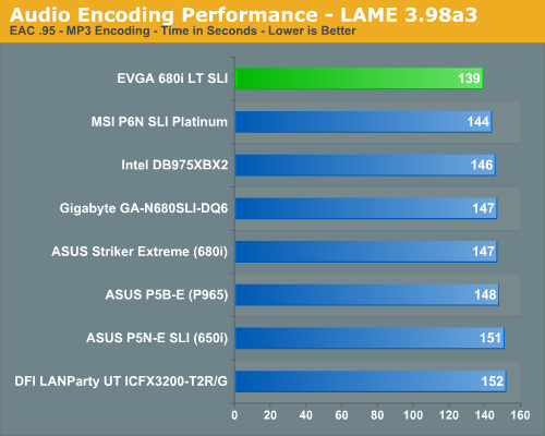
Our Plextor drive consistently took two minutes and nine seconds to read all sixteen tracks. This means our test systems were only utilizing one core during testing until the midway point of the extraction process where the drive speed was exceeding the capability of the encoder and required the use of a second thread.
Previously in the media encoding tests, the more intensive CPU and storage system tests seemed to favor the 975X over the P965/NV650i-680i/RD600 when running at the same memory timings. However, we are starting to notice a pattern in the latest NVIDIA releases where this is no longer the case, especially with 1T settings enabled on the NVIDIA chipset boards. We are currently retesting all of our NVIDIA boards with 1T settings as the latest BIOS releases are now offering stable 1T operation at DDR2-800 in our experience. While the overall differences are minimal in the grand scheme of things, 1T performance can make a slight difference in overall system performance. Our latest BIOS from MSI finally allows stable 1T operation with the initial test results equaling 136 seconds in this benchmark.
File Compression Performance
In order to save space on our hard drives and ensure we had another CPU crunching utility, we will be reporting our file compression results with the latest version of WinRAR that fully supports multi-treaded operations and should be of particular interest for those users with dual core or multi-processor systems. Our series of file compression tests utilizes WinRAR 3.62 to compress our test folder that contains 444 files, ten subfolders, and 602MB worth of data. All default settings are utilized in WinRAR along with our hard drive being defragmented before each test.
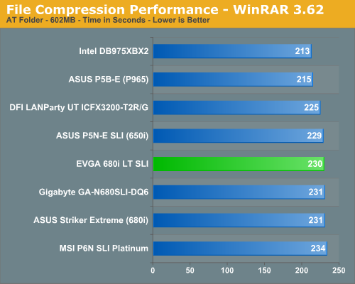
In a complete reversal of the other application results we see our EVGA board finishing near the bottom (all of the NVIDIA chipset boards are nearly tied). We see the Intel P965 and 975X chipsets leading once again as both seem to thrive in this CPU intensive task. The DFI RD600 board finishes in the middle of the pack. Historically, the NV Intel chipsets have not done well in this test due to CPU throughput being lower than the Intel chipsets. Changing our memory timings did not really affect the results overall although the EVGA board scores improved by 10 seconds with 1T enabled. In this particular test of CPU crunching power (which also makes use of a lot of memory bandwidth), the Intel chipsets win hands down.
Standard Gaming Performance
As usual, gaming performance was tested with a variety of current games. We ran benchmarks with our standard 1280x1024 resolution without antialiasing enabled (and generally without anisotropic filtering, though that varies by game). Given the number of users that run 19" LCDs these days, 1280x1024 represents one of the most commonly used resolutions. We could certainly increase the amount of eye candy being displayed in most of the games, but as this is a motherboard benchmark we aren't particularly interested in maxing out the graphics cards.
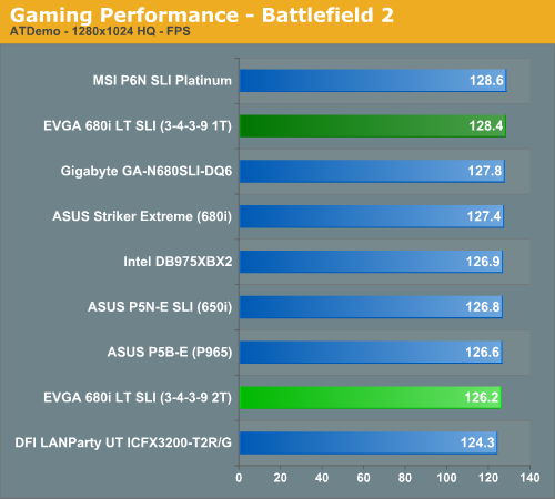
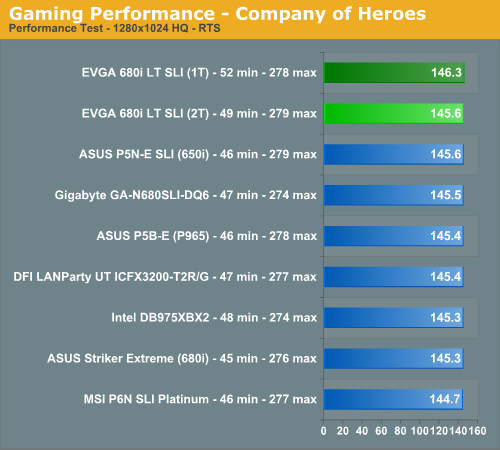
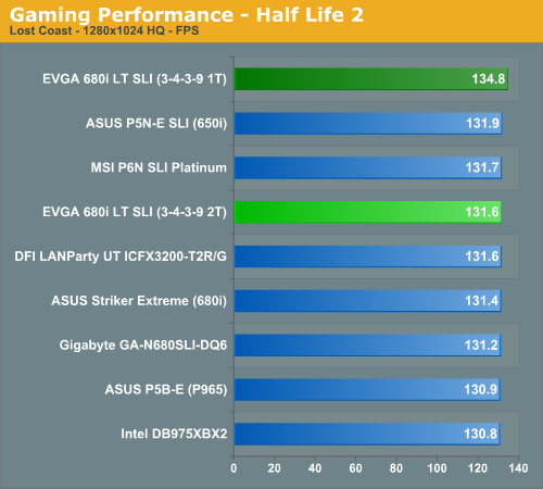
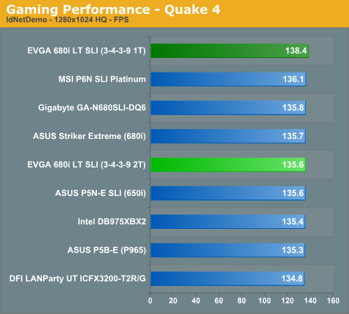
It's basically a toss up as to which chipset you select for a gaming machine. All of the results are very close and during actual game play we could not tell the difference between any of the boards. Our EVGA board finishes near the top in each test with a 2T command rate enabled and first in three tests with 1T enabled. While there is a measurable difference in the benchmarks, actual game play is the same - the largest performance increase from 1T is still only 2.5% in Half-Life 2. However, we will always take advantage of any opportunity to improve our system's performance.
We did not experience any issues during testing or during game play with the EVGA board at stock settings. We did encounter the dreaded NF4_DISP.DLL error while our system was overclocked with the E6600 processor at 9x425FSB. However, after removal/reinstallation of the video drivers along with the deletion of a particular registry key that NVIDIA suggested might be the culprit, we have not experienced any further issues. We generally play over a dozen different games for at least a couple of hours on each board to ensure there are no issues such as overheating, stuttering, or network issues when playing online with a various combination of components.
We will have a full selection of SLI game results along with a couple of new benchmarks in our next review. In the meantime, we did not find any noticeable differences in 8800GTX SLI performance between the 680i and 650i chipsets up to a resolution of 1920x1200 in games. The 3DMark06 synthetic benchmarks did show differences up to 6% but for the majority of gamers the differences in SLI performance between the two chipsets is negligible in actual game tests. It is only when you crank up the resolution to 2560x1600 or increase AA/AF settings that the dual x16 PCI Express capability on the 680i chipsets performs better than the dual x8 PCI Express setup on 650i.
Disk Controller Performance
The AnandTech iPeak test is designed to measure "pure" hard disk controller performance, and in this case, we keep the hard drive as consistent as possible while varying the hard drive controller. The idea is to measure the performance of each hard drive controller with the same hard drive.
We play back our raw files that are recorded I/O operations when running a real world benchmark - the entire Winstone 2004 suite. Intel's iPeak utility is then used to play back the trace file of all I/O operations that took place during a single run of Business Winstone 2004 and MCC Winstone 2004. The drive is formatted before each test run and a composite average of three tests on each controller interface is tabulated in order to ensure consistency in the benchmark.
iPeak gives a mean service time in milliseconds; in other words, the average time that each drive took to fulfill each I/O operation. In order to make the data more presentable, we report the scores as an average number of I/O operations per second so that higher scores translate into better performance. The resulting scores are useful for comparing "pure" performance of the storage controllers in this case.
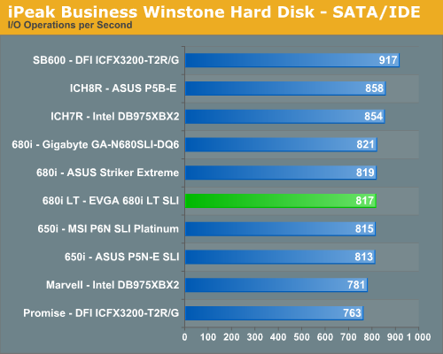
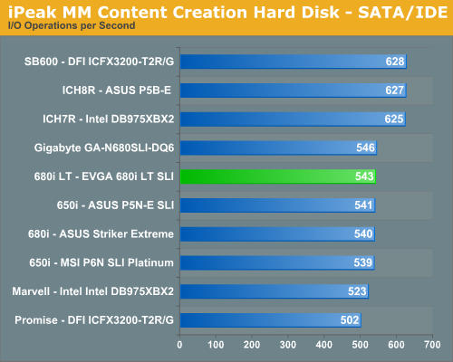
The performance patterns hold steady across both Multimedia Content I/O and Business I/O with the SB600 outperforming the Intel ICH7R, Intel ICH8R, and NVIDIA 680i/650i chipsets in our non-RAID tests. The Promise controller on the DFI board is the slowest of all solutions with the Marvell controller on the Intel 975X performing only slightly better. The 680i and 650i MCP chipsets are different but their disk performance in our tests is similar. We also ran RAID 0 and RAID 5 tests on each controller with the results being in favor of the 680i MCP by around 2% over the 680i LT MCP in these particular benchmarks. Although our NVIDIA boards generally score lower in these "pure" throughput tests, we find their actual performance in disk intensive applications are generally equal to or better than the other solutions.
Power Consumption
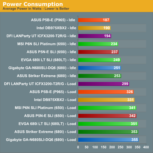
Our power consumption numbers are based on our test setup for this article that consists of an MSI 8800GTX video card and our boards have C1E/EIST turned off. The 680i boards lead all in power consumption but the 680i LT SLI is close behind with the LT certainly not meaning Lite in the way of power consumption. The P965 consumes the least amount of power at idle but around 10% more than the RD600 at load. The 975X still offers a decent level of power conservation compared to the other chipsets even though it is getting long in the tooth.
Overclocking
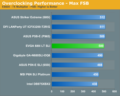
As we mentioned earlier in the article, the overclocking capability of the EVGA board has been neutered to some degree by the limited voltages and options available in the BIOS. Maybe we were just unlucky with our processor choices but this board had enough FSB holes that we thought about using it to whip up a few Swiss cheese sandwiches. After speaking with NVIDIA, we expect the overclocking capabilities of this chipset to vary based upon the luck of the draw when purchasing a board. Of course this is true of any component but it will be interesting to see the results of this latest effort by NVIDIA once the boards are in the hands of owners.
We believe their target is for consistent performance in the 450FSB to 475FSB range and anything above that will be icing on the big green cake. This will be disappointing to users who end up with a board that performs lower than our retail box sample but overclocking is never guaranteed. We will be purchasing a retail board from Newegg shortly to compare against our current board and will update our results if they are significant. Considering that there's a good chance the 680i LT boards are simply using rejected 680i chipsets - chips that couldn't run at higher FSB settings - we would advise caution for anyone looking to get an optimal overclocking platform.
We also found that during overclocking we had to set our CPU voltages a little higher than on the other boards to attain the same or better overclocks. We experienced this with the MSI 650i board and it was generally due to tighter memory/chipset timings in order to improve the performance of the board at stock speeds. Overall, our overclocking experiences were very good and the results of our tests show a board that is still very capable although certainly less than what we believe it is capable of with an enthusiast level BIOS.
First Impressions
This is our first look at the new 680i LT SLI chipset - or maybe we should say it is a slightly enhanced/revised/rescued 680i chipset. NVIDIA's goal was to offer similar performance and features of the 680i chipset specifically targeted to the "extreme" gamer but at a reduced price point. Did they achieve this goal? Yes and no to be quite honest.
After working with the EVGA 680i LT SLI board for a few weeks we have come to grudgingly accept its limitations while at the same time being impressed by its overall performance and quality. However, the work that NVIDIA's engineers or accountants did to ensure cost reductions and the neutering of the board's BIOS so it does not fully compete with the 680i boards still leaves us a little frustrated and annoyed.
Of course our frustration could be caused by several factors outside of NVIDIA's control, like reading the current news without a sense of humor or good cup of coffee nearby or being holed up in the test lab days on end without access to sunlight or McDonald's. However, after spending a bright sunny morning at McDonald's consuming a pot of coffee while watching Comedy Channel, we still think a couple of our frustrations with this board are justified.
Our first frustration is with the pricing scheme listing this board at $199. Sure this is $50 less than the suggested MSRP for the EVGA 680i board, but the last time we checked online that board was selling for around $199~$209 with rebate. There is no doubt in our minds what decision we would make between the two boards for an extra $10 or $15. We expect the price of the 680i LT SLI boards to also come in lower than the MSRP (currently at $174.99 with rebate), but it would have to be quite a bit lower for us to recommend saving a bit of money at the cost of an extra Ethernet port, additional USB ports, and a full-featured BIOS.
This leads us into the $199 price target. Except for SLI technology and somewhat asynchronous memory capability, what feature set or capability does this board have that others in this price range do not? [Crickets chirping...] Based on feature sets, pricing, and overall performance we think the MSI P6N SLI Platinum or the ASUS P5N32-E SLI Plus (full reviews coming shortly) offer a more compelling choice if you want NVIDIA SLI technology or would rather have a chipset solution that offers a greater degree of memory flexibility than what Intel provides currently.
Our second frustration is with the cost cutting - or more importantly cutting of corners based upon the market sector this board is currently targeting. Our press release materials state this chipset and in particular this board are "for extreme gamers who like to push their CPU and memory components to the next level". We can forgive the single network connection and to a certain degree (just barely) the dropping of two USB ports in order to save costs. However, we know a significant amount of gamers who would want both if given the choice and other boards at this price point offer it.
Our main issue is the neutering of the BIOS and this is an area where we feel NVIDIA contradicts itself. How can the "extreme gamer" push their CPU and memory components to the next level if the lack of BIOS options are hindering your ability to do what is being advertised? Everything about the construction of this board from its quality component selection to six-layer design screams of a performance capability that the BIOS does not live up to in its initial release.
As a customer of this board, after reading the press materials I would expect additional voltage options such as FSB VTT, GTL Ref, MCP, and HT along with additional voltage settings in the key areas of SPP, FSB, and memory options in order to take my components to the next level. Improving Vdroop with quad core processors and reducing the amount of FSB holes so we are not always thinking about cheesy goodness would be welcome improvements for both the gamer and overclocker.
Oh, and by the way, having full nTune compatibility, proper fan speed support for the chassis fans, and a passive cooling solution (or at least temperature based fan control on the chipset fans) so the "extreme gamer" can hear the action and not the board would be additional pluses. Other features such as LinkBoost and EPP capability up to DDR2-1200 would also be a nice addition for those looking to push their components. The board already supports DDR2-800 EPP profiles; why not toss in full support?
Of course by this point you have just designed a feature rich but limited options 680i board that probably would severely limit your high-end sales, something NVIDIA is desperately trying not to do. If you sense that we are slightly frustrated and annoyed, you would be right, but now for the good stuff.
This board, even with its BIOS and certain feature limitations, performed admirably and was a pinnacle of stability throughout our testing regimen. The board design, quality component choices, performance, and lack of BIOS compatibility issues is a testament to excellence by the engineering group at NVIDIA. This board has been running practically 24/7 since we received it, with a wide variety of components and without a real issue to date. The days of garbled sound with SLI enabled, data corruption with RAID arrays, USB issues, and poor quad core performance seem to be a distant memory when using this board. In fact, other than the differences mentioned above, it's almost just like running a 680i board - fancy that.
We have probably been a little too harsh on NVIDIA but with the right BIOS, a couple of minor layout changes, and a better price point this is the 680i board we have wanted for a long time. It's a shame really, but EVGA does appear to be targeting lower prices (currently coming in at $175 after rebate at some vendors). It's still priced awfully close to the 680i boards and too far above some very good 650i SLI boards for us to whole-heartedly recommend it, but it does appear to fill a niche. The board itself was a breath of fresh air and stood out from the crowd from an overall performance and stability viewpoint, so the non-extreme crowd should be very happy with this new option.
We feel like NVIDIA took the right path in their decision to market a performance oriented board in the $150~$200 price range but when compared to other solutions the engineers should have skipped the BIOS neutering process. The majority of issues we noted about the board can be overlooked to a certain degree due to the board's strengths. However, to play in this market sector you need an option rich BIOS, something this board does not have. That is the greatest mistake of all considering this is one of NVIDIA's greatest strengths, and we can only hope this will be rectified via a BIOS update.


