Original Link: https://www.anandtech.com/show/8239/update-on-samsung-850-pro-endurance-vnand-die-size
Testing Samsung 850 Pro Endurance & Measuring V-NAND Die Size
by Kristian Vättö on July 7, 2014 1:20 PM EST
Last week Samsung announced the 850 Pro, which is the first mainstream SSD to utilize 3D V-NAND. We already reviewed the drive and covered the fundamentals of V-NAND in detail but there is one thing I did not have the time to test: endurance. The most promising aspect of V-NAND is its increased endurance and Samsung has claimed endurance of up to ten times of 2D NAND. However, the 850 Pro is only rated at 150TB, which is twice the rating of 840 Pro, so I wanted to dig deeper and determine the endurance rating in terms of program/erase cycles.
To calculate the P/E cycles, I used a method similar to what we used with the SSD 840 two years ago. Basically, I wrote 128KB sequential data (QD1) to the drive and wrote down the necessary SMART values as well as the average throughput after every test. After repeating the test over a dozen times, I had enough data to figure out the P/E cycle count.
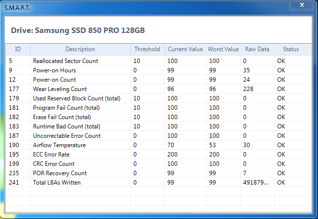
The Wear Leveling Count (WLC) SMART value gives us all the data we need. The current value stands for the remaining endurance of the drive in percentage, meaning that it starts from 100 and decreases linearly as the drive is written to. The raw WLC value counts the consumed P/E cycles, so if these two values are monitored while writing to the drive, sooner than later we will find the spot where the normalized value drops by one.
I found that the current WLC value drops by one after 60 P/E cycles (I ran the test over multiple WLC drops), which suggests that the WLC will drop to zero after 6,000 P/E cycles. In other words, the V-NAND in 850 Pro is good for 6,000 P/E cycles, which is twice the cycle count of modern 2D MLC NAND but quite far away from Samsung's "ten times the endurance" claims. Either Samsung is using lower binned parts in the 850 Pro (i.e. saving the 30,000 P/E cycle parts for enterprise drives) or the WLC value has artificially been limited to ensure that enterprises do not use the 850 Pro and pay the premium for the 845DC EVO/Pro instead. I am thinking it is more of the latter because the enterprise drives bring home much higher profits and of course Samsung wants to make sure that the 850 Pro is not used outside the client environment.
Once WLC reaches zero or one, it is generally a good idea to replace the drive as it may no longer be reliable. However, that does not mean that the drive will immediately fail -- according to JEDEC spec the P/E cycle rating is with one-year data retention, meaning that there can still be plenty of life left. The Tech Report's endurance testing gives a good picture of how much you can write after the WLC drops to zero, although personally I would still replace the drive ASAP because there is no guarantee that each drive performs similarly (remember, NAND is binned for endurance so there can be differences).
| SSD Lifetime Estimation | ||||
| 128GB | 256GB | 512GB | 1TB | |
| Raw NAND Capacity | 129GiB | 258GiB | 516GiB | 1032GiB |
| NAND P/E Cycles | 6,000 | |||
| Raw NAND Endurance | 755.9TiB | 1,511.7TiB | 3,023.4TiB | 6,046.9TiB |
| Lifespan with 20GiB of Host Writes per Day with 1.5x Write Amplification | 35.34 years | 70.68 years | 141.37 years | 282.74 years |
| Lifespan with 100GiB of Host Writes per Day with 3x Write Amplification | 7.07 years | 14.14 years | 28.27 years | 56.55 years |
| Drive Writes per Day with 5x Write Amplification | 1.10 | 1.10 | 1.10 | 1.10 |
The above table gives a good summary of how durable the 850 Pro really is. Even if you write 100GiB (GB in Windows is really GiB, i.e. 1024^3 bytes) per day with a write amplification of three, the smallest 128GB model will last for over seven years. 100GiB per day is very rare in a client environment and to be honest I can only see this applying to some high-end media professionals that use the drive for production purposes. On the other hand, media professionals will likely spring for a larger capacity anyway as 128GB might not even be capable of holding the data of one project. For a more typical user there is absolutely nothing to worry about as the 850 Pro will likely outlive the rest of the components.
Of course, there is still the 150TB write limitation on the warranty. That figure is based on host writes, so it applies even if you are only writing sequential data with low write amplification. Samsung did, however, tell me that they can make exceptions as long as the drive is used in client environment, meaning that the purpose of the endurance rating is mostly to make sure that the 850 Pro is not used in write intensive enterprise applications.
Testing Write Amplification
In addition to testing the endurance, I decided to see what the worst-case write amplification looks like. The test regime is similar to the endurance testing but the writes are 4KB random (QD32) to illustrate the worst possible scenario for the drive. Unfortunately, Samsung's SMART values do not report total NAND writes like Intel does, but the raw Wear Leveling Count basically gives us NAND writes in increments of the capacity of the drive (one P/E cycle = 129GiB of NAND writes for the 128GB drive). I recorded the Wear Leveling Count as well as the Total LBAs Written (i.e. host writes) value while writing 4KB random data to the drive.
| Worst-Case Write Amplification | |
| Host Writes | 493.9GiB |
| P/E Cycles Consumed | 42 |
| Approximate NAND Writes | 5,418GiB |
| Observed Write Amplification | 10.97x |
About 10x worst-case write amplification is fairly typical for a moden client SSD. Fortunately the days of +100x write amplification are over and under common client workloads the write amplification will usually stay below 2x.
| Worst-Case Endurance | ||||
| 128GB | 256GB | 512GB | 1TB | |
| Write Amplification | 11x | |||
| Total Bytes Written (TBW) | 68.7TiB | 137.4TiB | 274.9TiB | 549.7TiB |
| Drive Writes per Day for 5 Years | 0.43 | 0.43 | 0.43 | 0.43 |
The table above is just to show how the 850 Pro would bear in worst-case scenario that may be relevant to some enterprise users. I will be putting the 850 Pro through our enterprise test suite to see how it stacks up in terms of performance but especially with added over-provisioning, I can see the 850 Pro being viable for some read intensive enterprise workloads.
V-NAND Die Size: Bigger Than What We Initially Thought
In our 850 Pro review, I did some calculations to estimate the die size of the second generation V-NAND based on the first generation V-NAND. As some of our clever readers pointed out, the die size does not scale perfectly with the die capacity because the peripheral circuitry cannot be scaled as aggressively as the capacity can be. As a result, my initial estimation ended up being way too small because I did not take the scaling of the peripheral circuitry into account.
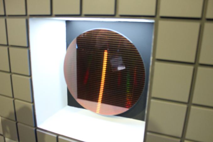
Unfortunately, Samsung would not disclose the die size during the Q&A at the SSD Global Summit so I had to seek for an alternative way to figure out the correct die size. In the showroom, Samsung had the second generation 32-layer V-NAND wafer, which actually gives us everything we need to calculate a fairly accurate estimation of the die size.
The picture on top shows what the wafer looks like. It does not look any different from the typical 2D NAND wafer, which should not be a surprise given that the change happened deep inside. And no, the V-NAND wafer is not thicker than any normal wafer (at least not by eye) because the V-NAND stack is still in the order of microns.
As for the die size, I calculated 44 dies in the vertical direction, which means that with a 300mm wafer the depth of a single die is approximately 6.8mm.
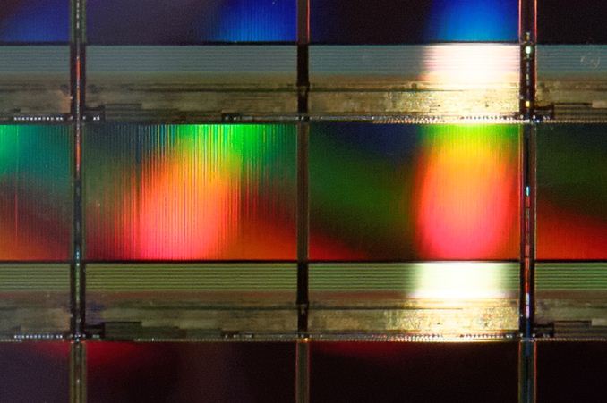
Courtesy of PC Perspective
To figure out the width of the die, you can either count the dies in the horizontal direction or go with the lazy route and just calculate the proportion of the depth and width. Allyn Malventano from PC Perspective was able to grab this awesome photo of the die itself, so I used the ruler tool in Photoshop to measure the size of the die along both X and Y axes and it appears that the width of the die is about 2.05 times its depth (note that it is a two-plane design). In other words, the die size is around 6.8mm x 14.0mm, which works out to be 95.4mm2.
| NAND Die Comparison | ||||
| Samsung 1st Gen V-NAND | Samsung 2nd Gen V-NAND | Micron 16nm NAND | Toshiba A19nm NAND | |
| Die Capacity | 128Gbit | 86Gbit | 128Gbit | 64Gbit |
| Die Size | 133mm2 | ~95.4mm2 | 173mm2 | 94mm2 |

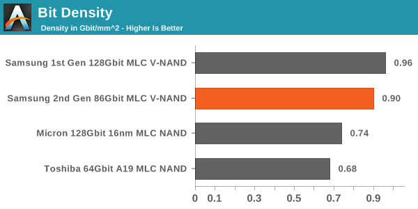
Here is an updated bit density graph. Even with the updated, larger die size, V-NAND is noticeably denser than 2D NAND, although the first generation appears to be more dense. I am guessing the smaller die size is better for yields (larger chips have higher probability of manufacturing errors), which makes the second generation more cost efficient despite the slightly lower density.


