Original Link: https://www.anandtech.com/show/964
Intel's 0.09-micron Process - More Details Emerge
by Anand Lal Shimpi on August 13, 2002 4:02 AM EST- Posted in
- CPUs
There has been a lot of talk about AMD's forthcoming Hammer processor but very little time is devoted to its imminent competitor - Prescott. Intel's Prescott core will be a relatively major upgrade to the Pentium 4 platform; the chip will bring higher clock speeds, a 1MB L2 cache, Hyper Threading and new instructions to the Pentium 4. Many of these enhancements will be made possible through the use of a new manufacturing process for the transistors that make up the Prescott core.
As mentioned in Intel's last quarterly report, over 50% of Intel's processor shipments are of 0.13-micron (130nm) CPUs such as the newest Pentium 4s. Intel's Prescott core, due out in the second half of next year, will be made on Intel's 0.09-micron (90nm) process. This new process is much more than a "simple die shrink" and actually contains a number of improvements, some of which we never expected Intel to be introducing this early.
Today Intel is sharing some more information about their 90nm process, expanding on what they revealed in March. Manufacturing based on the 90nm process has already commenced; if you'll remember back to our story from March, Intel has produced functional SRAM silicon based on their 90nm process. Obviously producing working SRAM (cache) silicon is not nearly as complicated as producing other parts of a CPU, but the bottom line is that the process is working as expected and they're meeting internal goals for it.
This is a welcome change from some of the dismal reports we've seen elsewhere about transitioning to smaller manufacturing processes. AMD's move to 0.13-micron was delayed and as of last quarter TSMC is only shipping around 1% of their parts on a 0.13-micron process. Intel has been able to extend a performance lead over the competition in recent times and part of the reason for this has been their lead in manufacturing capabilities.
By the end of this year Intel will have Prescott samples produced on the 90nm process sampling to partners, and by the time the second half of 2003 comes around Intel will be shipping 90nm parts in volume. Although the first 90nm chips are far away from being in even our hands, we're able to give you a glimpse of what to expect down the road based on Intel's announcements today.
A Very Cache-Friendly Process
One of Intel's biggest accomplishments with their 90nm process is an incredibly high cache density. In their March announcement, Intel introduced the world's highest capacity SRAM chip (6.5MB) on this 90nm process and its significance extends far beyond bragging rights.
 |
 |
|
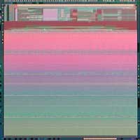
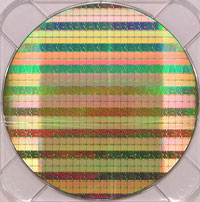
A 52Mbit SRAM chip manufactured on Intel's 90nm process (left). All parts built on Intel's 90nm process will be built on 300mm/12" wafers. This wafer of 90nm chips is composed of 330 billion transistors (right). |
|
As we mentioned before, Prescott will be home to a 1MB L2 cache, which is very impressive for a desktop chip. It wasn't too long ago that 1MB caches were reserved to server chips alone, but with their 90nm process Intel will be able to bring large L2 caches to the desktop. And they will need to in order to offer performance competitive to AMD's Hammer; with the Hammer's on-die memory controller, memory accesses can happen much faster meaning that the more often Prescott has to go to memory to fetch data, the more often Hammer will be faster in comparison. Having a very large L2 cache reduces the frequency Prescott will have to go to main memory for most applications without resorting to an on-die memory controller.
If Intel's desktop chips will get a 1MB L2 cache, what about their server solutions? It has been well known that Intel's Madison processor (third generation derivative of Itanium) would have a massive 6MB on-die L3 cache on a 0.13-micron process, but armed with Intel's 90nm process the Montecito core (fourth generation Itanium) will boast an incredible 12MB on-die L3 cache using close to 800 million of these 90nm transistors.
But being able to put larger caches on-die while taking up as little space as possible is just one of the feathers in Intel's 90nm cap…
Straining Silicon
The most interesting part of Intel's 90nm announcement today is the commitment to strained silicon technology. To understand the benefits of strained silicon you first have to understand some of the fundamental issues with transistors.
Simply put, you want transistors to be able to pass as much current as possible when they're switched on and to pass no current when they're switched off. Unfortunately we don't live in a perfect world and transistors don't always behave as they should. Technologies such as Silicon on Insulator (SOI) help stop current from flowing when it shouldn't (leakage current) and technologies such as Strained Silicon help increase the amount of current that's allowed to flow when it's needed (drive current).
We've already explained how Silicon on Insulator works and both AMD and Intel have committed to using the technology; AMD will be first to market with SOI through their Hammer parts, while Intel will introduce SOI with their 65nm process in 2005.
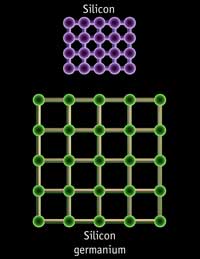
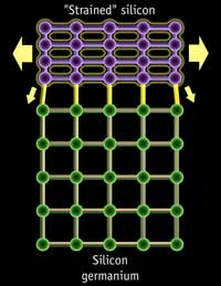
Strained Silicon works by effectively stretching the silicon in the channel region of the transistor. The engineers at Intel's fab facilities don't sit there and pull on both ends of the silicon in order to get it to stretch; rather they place the silicon on top of a substrate whose atoms are already spaced further apart than the silicon that needs to be stretched. The result of this is that the silicon atoms on top of the substrate will stretch to match the spacing of the substrate below, thus "stretching" the silicon in the channel.
 |
 |
|
Silicon
is "strained" by using a substrate of more widely spaced atoms
below the silicon channel of a transistor. (Images courtesy of IBM)
|
|
With more well spaced silicon atoms, electrons can now flow with less resistance in the channel meaning that more current can flow through the channel when needed. The end result is a 10 - 20% increase in drive current, or the current flowing through the channel of the transistor.
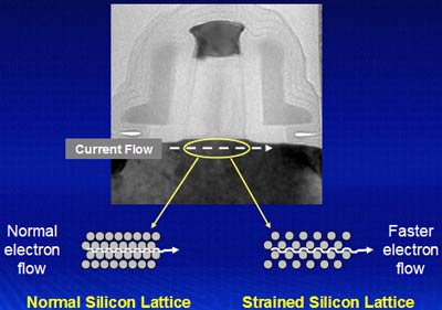
Intel claims that their Strained Silicon technology has no real downsides (unlike competing solutions) other than its 2% increase in manufacturing costs. Intel's 90nm process will make use of Strained Silicon technology to improve the performance of their 90nm transistors.
Getting Ready for Prescott - The 7th Layer
All of Intel's 0.13-micron parts presently employ 6 metal layers using copper interconnects to optimize circuit density and manufacturing cost; with the 90nm manufacturing process Intel has decided to add a 7th metal layer to allow for ~100M+ transistor designs such as Prescott and Montecito to be manufactured in the most efficient way possible.
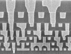
Can you count the 7 metal layers?
Some of the other features of Intel's 90nm process are beyond the scope of this article but include:
- 1.2nm gate oxide thickness (thinnest gate oxide in the industry)
- 50nm gate length initially, scaling down to even smaller gate lengths over the next two years (compared to 70nm gate lengths initially on the 0.13-micron process and currently 60nm)
- A new low-k Carbon-doped oxide dielectric to reduce wire-wire capacitance (thus reducing power)
The results of these improvements are of course, higher clock speeds and lower operating voltages. The first 90nm transistors will operate at a 1.20V and eventually scale down to even lower voltages; this should give you an idea of the core voltages you can expect to see on Prescott, depending on clock frequency of course.
Productizing 90nm - What does this mean to you?
All of this talk of technology is great and all but when can you expect to see based on Intel's 90nm process as we move on into next year?
For starters, Intel will be sampling 90nm based parts by the end of this year. But as a change of pace, instead of the mobile arena being the first to enjoy a new manufacturing process, it will be the desktop and server sectors that get a taste of Intel's 90nm technology first. The reason for this change of tradition is because Intel will be phasing the Pentium 4 out of the mobile market and concentrating on ramping up Banias to take over the throne in that sector. Banias will debut early next year on a 0.13-micron process and it will be a little while before it gets a 90nm shrink as well.
Instead, you can expect to see a 90nm Xeon part for low-power and low-heat blade server solutions as well as a potential 90nm derivative of the Northwood core.
Then there's the obvious 90nm solutions - Prescott and Montecito. While Prescott will definitely see more of our time than the 4th generation Itanium successor, both will drive Intel's 90nm process to its limits. A mass production ~100M transistor Prescott with a 1MB L2 cache and a 4GHz clock speed will be a reality in the very near future, and it will be made possible by the technology that Intel is announcing today.
Even Intel isn't sure exactly what product will bring 90nm technology to the mass-market first, but regardless of what it is, it will definitely have benefited from the extensive amounts of R&D investment Intel has put into their fabs.


