VIA Apollo Pro 133A Motherboard Roundup - July 2000
by Anand Lal Shimpi on July 21, 2000 5:31 AM EST- Posted in
- Motherboards
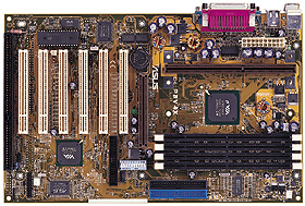
ASUS P3V4X
|
ASUS P3V4X Specifications |
|
| CPU Interface |
Slot-1
|
| Chipset |
VIA
Apollo 133A
VIA 694X North Bridge VIA 596B South Bridge |
| L2 Cache |
N/A
(on-chip)
|
| Form Factor |
ATX
|
| Bus Speeds |
66
/ 68 / 75 / 80 / 85 / 90 / 95 / 100 / 103 / 105 / 110
112 / 115 / 116 / 118 / 120 / 124 / 126 / 130 / 133 / 135 138 / 140 / 142 / 144 / 146 / 148 / 150 / 155 / 160 / 166 |
| Voltages Supported |
1.30v
- 1.80v (in 0.05v increments)
|
| Memory Slots |
3
168-pin DIMM Slots
|
| Expansion Slots |
0
AMR Slots
1 AGP Slot 6 PCI Slots (6 Full Length) 1 ISA Slot (1 Shared / 1 Full Length) |
| Onboard Audio |
N/A
|
| BIOS |
AWARD
Medallion BIOS 6.00
|
The ASUS P3V4X was our favorite board after the last roundup, but unfortunately we could not whole heatedly recommend it because it's gaming performance with the latest VIA GART driver at the time was horrible. Fortunately, VIA has released an updated GART driver that fixes the problems with the P3V4X (covered in detail here), allowing us to finally award it the Editor's Choice Gold Award that it deserved in the first place. But how would it stand up to the second wave of 133A boards? Well, let's see.
The P3V4X continues to be the best solution for overclockers, as it features a total of 32 FSB settings, and unlike other motherboards that claim support for an enormous amount of FSB settings, the P3V4X actually offers settings that can be useful to overclockers, especially when you’re overclocking an FC-PGA CPU.
The board features ASUS’ JumperFree setup and configuration utility that resides within the board’s AWARD "Medallion" BIOS setup. The Medallion BIOS is the result of the merger between Phoenix and AWARD about a year ago. What we get is a BIOS that looks and operates like a Phoenix BIOS, but includes all the features of an AWARD BIOS - not a bad combination at all.
Using the JumperFree setup you can adjust the memory clock, FSB frequency, and the voltage supplied to the CPU. The JumperFree setup will automatically select the AGP clock ratio based on your FSB selection in the BIOS, but if you want to adjust this option or any other setting manually, the P3V4X features its own set of override settings on the board that are controlled by a block of 10 dip-switches. Note that not all FSB frequencies are available when using the DIP switches on the board.
The ASUS P3V4X was once again one of the most reliable boards we tested, right up there with the AOpen boards. Fortunately, ASUS did not have to make any performance trade offs to achieve this feat.
One of our biggest complaints about the P3V4X is that ASUS chose to go with the 596B South Bridge instead of the highly integrated 686A Super South Bridge. This is quite disappointing since the 686A would help to cut down on the cost of the board while adding some additional functionality.
ASUS has actually addressed our South Bridge issue by releasing the successor to the P3V4X, the CUV4X. Unfortunately, the CUV4X was not available in time for this roundup, but it is quite similar to the P3V4X. The main differences are the use of the 686A Super South Bridge and a Socket-370 interface. It is based on the "new" 694Z North Bridge from VIA, which is functionally identical to the 694X, but features a different pin out so that motherboard manufacturers can use one PCB to support both the Apollo Pro 133A and the ProSavage PM133 (133A + integrated Savage 4 graphics).


0 Comments
View All Comments