AMD 760MP & Athlon MP - Dual Processor Heaven
by Anand Lal Shimpi on June 5, 2001 12:00 PM EST- Posted in
- CPUs
The importance of Cache Coherency
Imagine for a moment that you have a building with two programmers working. They are in adjacent cubicles and are working on the same project. Their manager is across the hall in another office and can see what the two are working on. Obviously it is necessary for the two programmers to communicate with one another so that they know what each other is doing. Assuming they can't talk, there are two ways for the programmers to communicate with one another. One way is by reaching around the cubicle and passing notes to one another; and the other way is to send a message to the manager and have him deliver it to the other programmer. Clearly, the first way is the most efficient and most appropriate. If you haven’t figured it out thus far, this is an example of the communication that must occur between two CPUs.
Now it is quite useful for one programmer to find out if the other one has a particular function already written, but it would require constant communication between the two, and as we already established, these two programmers don’t talk. This is another problem that MP systems encounter, how does one CPU know what is stored in the other CPU’s cache?
In most SMP systems, the individual CPUs monitor for requests across the FSB and return the data if it is present within the CPU’s cache. For example, let’s take a dual processor Athlon MP system with two Athlon MP CPUs: CPU0 and CPU1. First, CPU0 requests a block of data that is contained within main memory and not within CPU0’s cache or CPU1’s cache. The data is delivered from main memory, through the North Bridge, up to the CPU that requested it, in this case CPU0.
Then, CPU0 requests another block of data that is located within CPU1’s L2 cache. CPU1 is always monitoring (also called snooping) the FSB for requests for data; this time around, the data is in its cache and it sends it out. Now there are two ways of getting the data to CPU0: it can either be written to main memory by CPU1 and read by CPU0, or it can be transferred directly from CPU1 to CPU0.
 In
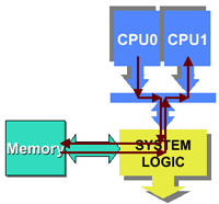
the case of a Shared Front Side Bus (see right), where all of the CPUs in a
MP system share the same connection to a
The Shared FSB and Point-to-Point FSB aren’t functions of the CPU; all the
Athlon MP can do is make sure it works with a particular protocol. Instead,
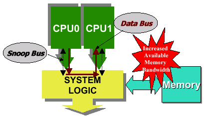
this is a chipset function, and in the case of the 760MP, it implements a Point-to-Point
bus protocol. This helps reduce memory bus traffic since all inner-CPU communication
occurs without even hitting the memory bus. For comparison’s sake, all MP chipsets
for Intel processors use a Shared FSB including the recently released i860 chipset
for the Intel Xeon. It is arguable whether or not the ability to direct all
snooping traffic internally within the

Another benefit of the Athlon MP’s EV6 FSB is that there are two unidirectional address ports (address in and address out) and one bidirectional data port in every EV6 bus link. This means that an Athlon MP can snoop for data it needs while fulfilling a data request at the same time. The Pentium 4’s AGTL+ FSB only has a single bidirectional address port and a single bidirectional data port meaning that addresses can only be sent to/from the processor at once, not simultaneously.
Taking our Athlon MP system out for another test, we have the following situation: CPU0 has a block of data in its cache, and CPU1 has the same data in its cache. CPU1 then changes the data that both processors have in their caches after which CPU0 attempts to read that data. At this point the copy of the data stored in CPU0’s cache isn’t the most recent copy; in fact it has been changed since CPU0 pulled it into its cache. Keeping the data in each CPU’s cache up to date, or coherent with one another, is what we mean when we refer to cache coherency.
There are only a couple major cache coherency protocols but many variants of them. By far the most common cache coherency protocol is known as write invalidate. Generally speaking, the write invalidate coherency protocol simply dictates which processor’s cache to invalidate the data in during the event of a coherency conflict. The invalidate function is one that takes place over the address bus alone, meaning that the EV6’s dual ported address bus comes in handy once again, allowing for a cache line invalidate and a data request to be executed simultaneously.
There are many forms of the write invalidate coherency protocol, the most common being a MESI protocol. The four-letter acronym stands for the four states (Modified, Exclusive, Shared or Invalid) that a cache line may take. The meanings of the four states are as follows:
Modified – The data in the line has been modified thus meaning that the copy in main memory is invalidated.
Exclusive – The only copy of the data is stored in this cache thus meaning that the copy in main memory is valid.
Shared – The data is in more than one processor’s cache and the copy in memory is valid.
Invalid – The data in cache is invalid.
The MESI protocol is present in the majority of x86 processors including the AMD K6, Intel Pentium III, Pentium 4 and Xeon. Even the PowerPC processor uses the MESI protocol.
The Athlon MP (including all previous Athlon variants and the Duron) uses a five-state MOESI protocol instead. The MOESI protocol adds another state known as the “Owned” state. This is a state that is triggered when the data being requested is in more than one processor’s cache and the data in one cache has been modified.
Implementing MOESI cache coherency is much more complicated than the basic four step MESI implementation and thus requires many more transistors to implement. However, it works perfectly with the Athlon MP’s Point-to-Point FSB’s dual address ports and actually increases bus efficiency.
The MOESI cache coherency protocol had been previously reserved for high-end server CPUs such as the Sun UltraSPARC II, but the Athlon actually debuted with it back in 1999.


0 Comments
View All Comments