HBM

Under the CHIPS & Science Act, the U.S. government provided tens of billions of dollars in grants and loans to the world's leading maker of chips, such as Intel, Samsung, and TSMC, which will significantly expand the country's semiconductor production industry in the coming years. However, most chips are typically tested, assembled, and packaged in Asia, which has left the American supply chain incomplete. Addressing this last gap in the government's domestic chip production plans, these past couple of weeks the U.S. government signed memorandums of understanding worth about $1.5 billion with Amkor and SK hynix to support their efforts to build chip packaging facilities in the U.S. Amkor to Build Advanced Packaging Facility with Apple in Mind Amkor plans to build a $2 billion advanced...
Micron to Launch HBM2 DRAM This Year: Finally
Bundled in their latest earnings call, Micron has revealed that later this year the company will finally introduce its first HBM DRAM for bandwidth-hungry applications. The move will enable...
14 by Anton Shilov on 3/27/2020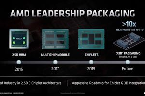
AMD Discusses ‘X3D’ Die Stacking and Packaging for Future Products: Hybrid 2.5D and 3D
One of AMD’s key messages at its Financial Analyst Day 2020 is that the company wants to remain on the leading edge when it comes to process node technology...
12 by Dr. Ian Cutress on 3/5/2020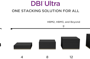
SK Hynix Licenses DBI Ultra Interconnect for Next-Gen 3DS and HBM DRAM
SK Hynix has inked a new broad patent and technology licensing agreement with Xperi Corp. Among other things, the company licensed the DBI Ultra 2.5D/3D interconnect technology developed by...
9 by Anton Shilov on 2/11/2020
Samsung Develops 12-Layer 3D TSV DRAM: Up to 24 GB HBM2
Samsung on Monday said that it had developed the industry’s first 12-layer 3D packaging for DRAM products. The technology uses through silicon vias (TSVs) to create high-capacity HBM memory...
11 by Anton Shilov on 10/7/2019
Samsung HBM2E ‘Flashbolt’ Memory for GPUs: 16 GB Per Stack, 3.2 Gbps
Samsung has introduced the industry’s first memory that correspond to the HBM2E specification. The company’s new Flashbolt memory stacks increase performance by 33% and offer double per-die as well...
25 by Anton Shilov on 3/20/2019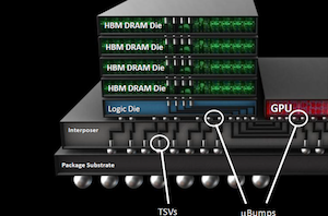
JEDEC Updates HBM Spec to Boost Capacity & Performance: 24 GB, 307 GB/s Per Stack
JEDEC this week published an updated version of its JESD235 specification, which describes HBM and HBM2 DRAM. The new version of the standard allows memory manufacturers to increase capacities...
15 by Anton Shilov on 12/19/2018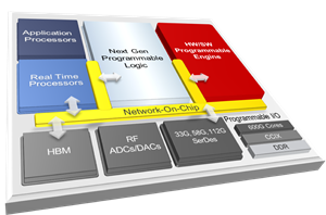
Xilinx Announces Project Everest: The 7nm FPGA SoC Hybrid
This week Xilinx is making public its latest internal project for the next era of specialized computing. The new product line, called Project Everest in the interim, is based...
16 by Ian Cutress on 3/19/2018
Samsung Starts Production of HBM2 “Aquabolt” Memory: 8 GB, 2.4 Gbps
Samsung this week announced that it had started mass production of its second-generation HBM2 memory code-named “Aquabolt”. The new memory devices have 8 GB capacity and operate at 2.4...
17 by Anton Shilov on 1/11/2018
SK Hynix: Customers Willing to Pay 2.5 Times More for HBM2 Memory
SK Hynix was the first DRAM manufacturer to start producing HBM Gen 1 memory in high volume back in 2015. However, the company is somewhat behind its rival Samsung...
23 by Anton Shilov on 8/4/2017
Hot Chips 2016: Memory Vendors Discuss Ideas for Future Memory Tech - DDR5, Cheap HBM, & More
Continuing our Hot Chips 2016 coverage for the evening, along with the requisite presentations on processors, several of the major players in the memory industry are also at the...
11 by Ryan Smith on 8/23/2016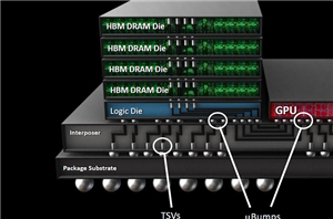
SK Hynix Adds HBM2 to Catalog: 4 GB Stacks Set to Be Available in Q3
SK Hynix has quietly added its HBM Gen 2 memory stacks to its public product catalog earlier this month, which means that the start of mass production should be...
43 by Anton Shilov on 8/1/2016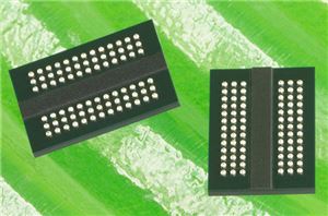
GDDR5X Standard Finalized by JEDEC: New Graphics Memory up to 14 Gbps
In Q4 2015, JEDEC (a major semiconductor engineering trade organization that sets standards for dynamic random access memory, or DRAM) finalized the GDDR5X specification, with accompianing white papers. This...
70 by Anton Shilov on 1/22/2016
JEDEC Publishes HBM2 Specification as Samsung Begins Mass Production of Chips
The high-bandwidth memory (HBM) technology solves two key problems related to modern DRAM: it substantially increases bandwidth available to computing devices (e.g., GPUs) and reduces power consumption. The first-generation...
42 by Anton Shilov on 1/20/2016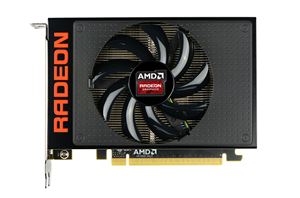
AMD Announces Radeon R9 Nano; mini-ITX Card Shipping September 10th
Back in June at AMD’s R9 Fury X/Fiji GPU launch event, the company unveiled that there would be four products based on Fiji. Fury X and Fury – which...
95 by Ryan Smith on 8/27/2015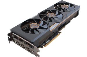
The AMD Radeon R9 Fury Review, Feat. Sapphire & ASUS
A bit over two weeks ago AMD launched their new flagship video card, the Radeon R9 Fury X. Based on the company’s new Fiji GPU, the R9 Fury X...
288 by Ryan Smith on 7/10/2015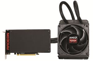
The AMD Radeon R9 Fury X Review: Aiming For the Top
Having launched last week and being reviewed today is AMD’s Radeon R9 Fury X, the company’s new flagship single-GPU video card. Featuring a fully enabled Fiji GPU, the R9...
458 by Ryan Smith on 7/2/2015
AMD Shows Off Dual-GPU Fiji Card At PC Gaming Show
Briefly announced and discussed during AMD’s 2015 GPU product presentation yesterday morning was AMD’s forthcoming dual Fiji video card. The near-obligatory counterpart to the just-announced Radeon R9 Fury X...
133 by Ryan Smith on 6/17/2015

AMD Teases Upcoming Video Card
Between Financial Analyst Day 2015, their briefing on High Bandwidth Memory, and now a carefully seeded hardware sample to DICE developer and uber guru Johan Andersson, AMD is making...
75 by Ryan Smith on 5/22/2015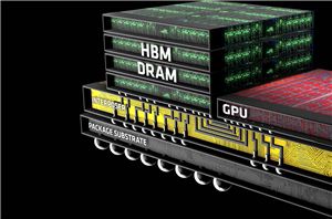
AMD Dives Deep On High Bandwidth Memory - What Will HBM Bring AMD?
Earlier this month at AMD’s 2015 Financial Analyst day, the company announced that they would be releasing their first High Bandwidth Memory-equipped GPU – the world’s first HBM-equipped GPU...
163 by Ryan Smith on 5/19/2015


