P55 Chipset - Quick Primer
by Gary Key on September 8, 2009 12:15 AM EST- Posted in
- Gary's First Looks
It Slices, It Dices. But Wait, There’s More!
Actually, there is not more. A couple of years ago rumors were floating around that Intel’s first Platform Controller Hub (PCH) would contain the latest in features like 6Gb/s SATA ports, USB 3.0, and full PCI Express 2.0 capabilities all at a price that even McDonald’s would be envious of when launched. Of course, you know rumors are usually just that, silly rumors.
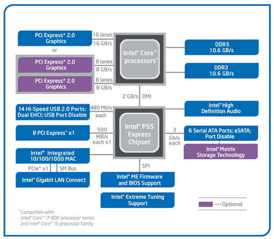
Instead, we end up with what I would conveniently call ICH10.1. Even Windows 7 agrees with us when loading drivers. Except that PCH is the new ICH, otherwise we are talking the same part, almost. There are a few minor differences between the P55 and ICH10R as we see below.
| AMD SB750 | Intel ICH10R | Intel P55 | |
| Additional PCI Express | None | 6 x1 PCIe 1.1 | 8 x 1 PCIe 2.0 |
| USB | 12 ports | 12 ports | 14 ports |
| SATA (300MB/s) | 6 ports | 6 ports | 6 ports |
| PATA | 2 channels | None | None |
| RAID* | RAID 0/1/5/10 | RAID 0/1/5/10 | RAID 0/1/5/10 |
| HD Audio Interface | Yes | Yes | Yes |
| Ethernet | Not Integrated | Intel Gigabit LAN | Intel Gigabit LAN |
| Northbridge Interface | 4 lane PCIe 1.1 | DMI 10Gb/s each direction, full duplex | DMI 10Gb/s each direction, full duplex |
The P55 gives you six 3 Gb/s SATA ports, 14 USB 2.0 ports, a Gigabit Ethernet MAC , HD Audio, and eight lanes of PCI Express 2.0 goodness all for $40. That price tag buys you two additional USB ports and two additional PCIe lanes over the $3 ICH10R. The PCI Express lanes are version 2.0 but Intel decided to limit their speed to PCIe 1.x specs at 2.5GT/s. Why? We think it is because the DMI link continues at 1GB/s in each direction, which means a decent 6Gb/s SAS/SATA RAID card and a few upcoming 6Gb/s drives (SSDs anyone) could easily saturate the link. The P55 and ICH10R both consume a little over 4.5W during normal operation. Considering the specifications on AMD’s new SB8xxx chipsets, it appears we have a PCH Gap brewing.
How is performance? We are still trying to reach a conclusion and asked Intel for additional information. Overall, the two chipsets are about even in actual usage that includes file transfers and application benchmarks. The synthetic programs like HDTach and HDTune tell another story but one that we do not trust. Iometer shows both controllers neck and neck with our WD VelociRaptors in RAID testing, but a slight nod to the ICH10R in single disk testing with our OCZ Vertex 120GB SSD. We will have results in the upcoming P55 motherboard roundups (three total) starting later this week.


24 Comments
View All Comments
Ryan Smith - Tuesday, September 8, 2009 - link
If it's anything like PCIe, then it would be using 8b/10b encoding. So 10Gb is 1GB, and since it's full duplex 1GB + 1GB = 2GB. At any rate I'm just fixing typos, Gary can tell you more.OSJF - Tuesday, September 8, 2009 - link
Ok, so that would be 250MByte/s, right?http://en.wikipedia.org/wiki/PCI_Express">http://en.wikipedia.org/wiki/PCI_Express
"a decent 6Gb/s SAS/SATA RAID card and a few upcoming 6GB/s drives (SSDs anyone) could easily saturate the link"
?!?
Even a decent 3Gb/s controller could reach 250Mbyte/s.
I'm really confused..... :)
JarredWalton - Tuesday, September 8, 2009 - link
I believe the DMI link runs at 1GHz, thus you could say it's a "1Gbps" link. However, it's also 16-bits wide, and a byte is 8 bits, so it's "2GBps". Then you have to account for the fact that it's really a full-duplex stream, so it's actually half that bandwidth in each direction -- 1GBps up and 1GBps down. (I think - I might have that figure wrong.) The SATA spec is 3Gbps but that's using 8/10 encoding so they're really 300MBps; 6Gbps will similarly be 600MBps.The net result is that the DMI interface is about the same as four PCI-E 1.x lanes (4 x 250MBps in each direction). A single 6Gbps SATA device could use 60% of that, so two SSDs running at 6Gbps would saturate the link. I suppose Intel could have the PCI-E lanes still run at a theoretical 2.0 spec, but they would never really get that bandwidth in practice. It's why PCI-E 2.0 off a Southbridge has never really made sense IMO.
R3MF - Tuesday, September 8, 2009 - link
1. what is manufacture process is the P55 chipset fabbed at?2. why doesn't AMD use HT to connect the NB and SB, seems very relevant given your reference to saturation potential in the P55?