Zotac ZBOX HD-ID11 Review: Next Gen ION is Better & Worse than ION1
by Anand Lal Shimpi on May 6, 2010 3:51 PM EST- Posted in
- GPUs
- Next Generation ION
- HD-ID11
- ZOTAC
- NVIDIA
The nForce 2 was one of the best chipsets to come out of NVIDIA. It was NVIDIA’s second attempt at a desktop chipset yet it cemented NVIDIA’s position as a leading provider of core logic in the market. Oh how much has changed since then.
Most of what made a chipset worthwhile is now integrated into the CPU. It used to be memory controller optimizations that kept chipsets afloat, but that’s no longer the case as all x86 processors now ship with an integrated memory controller. The performance differences between chipsets disappeared and all that was left was testing, validation and drivers, also known as the boring, expensive and time consuming aspects of chipset development.
NVIDIA has mostly abandoned the chipset business, focusing on opportunistic wins where possible. The most obvious example is with ION, its chipset/GPU for Atom based systems.
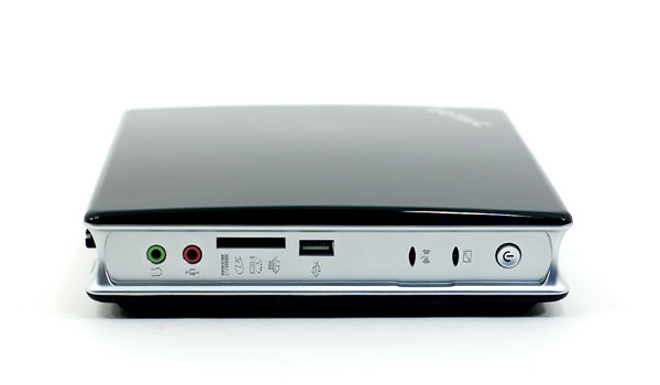
Last year we played with a number of ION systems and motherboards and were generally impressed. The platform made for a powerful little HTPC. Today we’re able to bring you a hands on performance preview of the first Next Generation ION box we’ve laid our hands on: the Zotac ZBOX HD-ID11.
Terms of Ndearment
CPUs connect to the outside world using proprietary bus interfaces. AMD uses Hyper Transport, while Intel previously used the AGTL+ FSB. In order to build a device that hangs off of this interface you need a license to use it. This is just an IP license to let you integrate the circuitry you need to communicate over that bus onto your silicon. It’s pretty commonplace.
Over the years Intel would update its FSB (Front Side Bus) specification, and it would threaten its chipset partners with revoking their license to the new version of the FSB unless they cooperated. Intel and VIA had a disagreement over this years ago that ended in VIA threatening Intel with CPU patents and the two coming to terms later on.
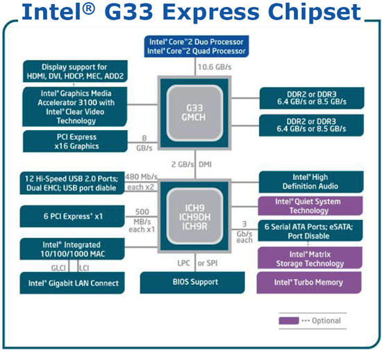
The old way of doing things, FSB between the CPU and the GMCH, DMI between the GMCH and ICH.
With Nehalem, Intel moved away from a parallel bus interface and introduced QPI (Quick Path Interconnect). This is a very high bandwidth point to point protocol designed for high end servers, workstations and desktops. It’s used in the Nehalem and Gulftown based Core i7s. NVIDIA said it had no interest in pursuing a QPI based chipset, so the issue of licensing never came up.
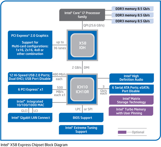
The new way, QPI between the CPU and IOH. DMI between the IOH and ICH.
A much lower bandwidth interconnect called DMI (Direct Media Interface) would be used for mainstream Nehalem/Westmere derivatives (e.g. Core i3, Core i5, LGA-1156 Core i7). Intel had used this interconnect in the past to connect parts of its chipsets together, but now it would be used to connect the CPU to a chipset.
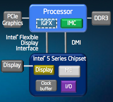
The other new way: DMI between the CPU and chipset.
With its own aspirations of getting into the GPU market, and no real need for NVIDIA’s allegiance, Intel enforced its license agreement and threatened a lawsuit if NVIDIA sold chipsets that used Intel’s DMI. NVIDIA argued that it was well within its rights to do so but didn’t want to risk it and stopped development on DMI chipsets pending the outcome of its lawsuit against Intel for violating the terms of the license agreement.
The ION Problem
While all of this was going on, Intel’s Atom platform started gaining momentum in netbooks and nettops. The netbook version of Atom used the old AGTL+ FSB to connect to its chipset, so NVIDIA could technically produce chipsets for it. Which is exactly what NVIDIA did. It was called ION (and later renamed to Atom + ION).
The latest version of Atom for netbooks/nettops, codenamed Pineview, integrates the memory controller and graphics core. Its only connection to the outside world is, you guessed it, a DMI link.
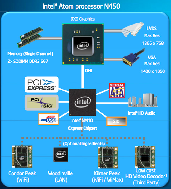
In a Pine Trail Atom system, the Pineview CPU connects to Intel’s NM10 Express chipset over this DMI link. With no license for DMI and no desire to push its luck, NVIDIA can’t offer a drop in replacement for the NM10 Express chipset.
Luckily, Intel’s NM10 Express Chipset includes four PCIe 1.0 lanes. A motherboard manufacturer could simply hang a low end, discrete GPU off of these PCIe lanes and you’d get a modern ION platform. And that’s what NVIDIA did for its Next Generation ION.
Meet NG-ION
NVIDIA’s Next Generation ION is a 40nm discrete GPU based on the GT218 core, it’s effectively the same GPU as a desktop GeForce 210 video card with some differing clock speeds. The nettop version uses 16 cores, while the netbook version uses 8 or 16 depending on the screen size.


While manufacturers can use all four PCIe 1.0 lanes coming off Intel’s NM10 Express chipset, most have chosen to use just one leaving the remaining lanes for things like WiFi. A single PCIe 1.0 lane can only provide 250MB/s of bandwidth in either direction, hardly enough for a modern GPU. It’s because of this limitation that the next-generation ION GPU could actually perform slower than the first ION.
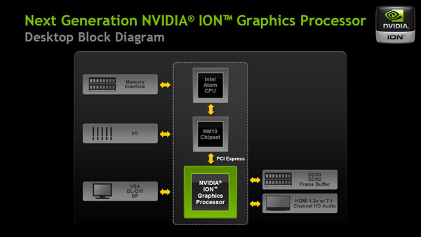
As a discrete GPU, the NG-ION comes with its own frame buffer: up to 512MB of DDR3 on a nettop. You also get full H.264 video decode acceleration and support for 8-channel LPCM audio over HDMI out.


40 Comments
View All Comments