NVIDIA's GeForce GTX 580: Fermi Refined
by Ryan Smith on November 9, 2010 9:00 AM ESTKeeping It Cool: Transistors, Throttles, and Coolers
Beyond the specific architectural improvements for GF110 we previously discussed, NVIDIA has also been tinkering with their designs at a lower level to see what they could do to improve their performance in conjunction with TSMC’s 40nm manufacturing process. GF100/GTX480 quickly gathered a reputation as a hot product, and this wasn’t an unearned reputation. Even with an SM fused off, GTX 480 already had a TDP of 250W, and the actual power draw could surpass that in extreme load situations such as FurMark.
NVIDIA can (and did) tackle things on the cooling side of things by better dissipating that heat, but keeping their GPUs from generating it in the first place was equally important. This was especially important if they wanted to push high-clocked fully-enabled designs on to the consumer GeForce and HPC Tesla markets, with the latter in particular not being a market where you can simply throw more cooling at the problem. As a result NVIDIA had to look at GF110 at a transistor level, and determine what they could do to cut power consumption.
Semiconductors are a near-perfect power-to-heat conversion device, so a lot of work goes in to getting as much work done with as little power as necessary. This is compounded by the fact that dynamic power (which does useful work) only represents some of the power used – the rest of the power is wasted as leakage power. In the case of a high-end GPU NVIDIA doesn’t necessarily want to reduce dynamic power usage and have it impact performance, instead they want to go after leakage power. This in turn is compounded by the fact that leaky transistors and high clocks are strange bedfellows, making it difficult to separate the two. The result is that leaky transistors are high-clocking transistors, and vice versa.
![]()
A typical CMOS transitor: Thin gate dielectrics lead to leakage
Thus the trick to making a good GPU is to use leaky transistors where you must, and use slower transistors elsewhere. This is exactly what NVIDIA did for GF100, where they primarily used 2 types of transistors differentiated in this manner. At a functional unit level we’re not sure which units used what, but it’s a good bet that most devices operating on the shader clock used the leakier transistors, while devices attached to the base clock could use the slower transistors. Of course GF100 ended up being power hungry – and by extension we assume leaky anyhow – so that design didn’t necessarily work out well for NVIDIA.
For GF110, NVIDIA included a 3rd type of transistor, which they describe as having “properties between the two previous ones”. Or in other words, NVIDIA began using a transistor that was leakier than a slow transistor, but not as leaky as the leakiest transistors in GF100. Again we don’t know which types of transistors were used where, but in using all 3 types NVIDIA ultimately was able to lower power consumption without needing to slow any parts of the chip down. In fact this is where virtually all of NVIDIA’s power savings come from, as NVIDIA only outright removed few if any transistors considering that GF110 retains all of GF100’s functionality.
Of course reducing leakage is one way to reduce power consumption, but it doesn’t solve NVIDIA’s other problems in hitting their desired TDP. Both NVIDIA and AMD base their GPU TDP specifications around “real world” applications and games, with NVIDIA largely viewed to be more aggressive on this front. In either case load-generating programs like FurMark and OCCT do not exist in AMD or NVIDIA’s worlds, leading both companies to greatly despise these programs and label them as “power viruses” and other terms.
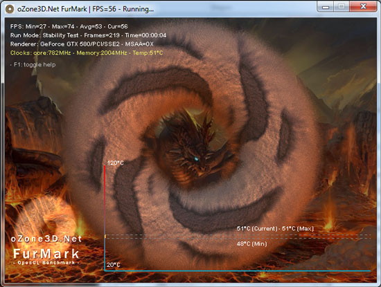
After a particularly rocky relationship with FurMark blowing up VRMs on the Radeon 4000 series, AMD instituted safeties in their cards with the 5000 series to protect against FurMark – AMD monitored the temperature of the VRMs, and would immediately downclock the GPU if the VRM temperatures exceeded specifications. Ultimately as this was temperature based AMD’s cards were allowed to run to the best of their capabilities, so long as they weren’t going to damage themselves. In practice we rarely encountered AMD’s VRM protection even with FurMark except in overclocking scenarios, where overvolting cards such as the 5970 quickly drove up the temperature of the VRMs.
For GTX 580 NVIDIA is taking an even more stringent approach than AMD, as they’ll be going after power consumption itself rather than just focusing on protecting the card. Attached to GTX 580 are a series of power monitoring chips, which monitor the amount of power the card is drawing from the PCIe slot and PCIe power plugs. By collecting this information NVIDIA’s drivers can determine if the card is drawing too much power, and slow the card down to keep it within spec. This kind of power throttling is new for GPUs, though it’s been common with CPUs for a long time.
NVIDIA’s reasoning for this change doesn’t pull any punches: it’s to combat OCCT and FurMark. At an end-user level FurMark and OCCT really can be dangerous – even if they can’t break the card any longer, they can still cause other side-effects by drawing too much power from the PSU. As a result having this protection in place more or less makes it impossible to toast a video card or any other parts of a computer with these programs. Meanwhile at a PR level, we believe that NVIDIA is tired of seeing hardware review sites publish numbers showcasing GeForce products drawing exorbitant amounts of power even though these numbers represent non-real-world scenarios. By throttling FurMark and OCCT like this, we shouldn’t be able to get their cards to pull so much power. We still believe that tools like FurMark and OCCT are excellent load-testing tools for finding a worst-case scenario and helping our readers plan system builds with those scenarios in mind, but at the end of the day we can’t argue that this isn’t a logical position for NVIDIA.
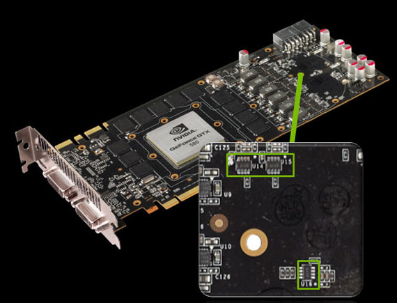
Power Monitoring Chips Identified
While this is a hardware measure the real trigger is in software. FurMark and OCCT are indeed throttled, but we’ve been able to throw other programs at the GTX 580 that cause a similar power draw. If NVIDIA was actually doing this all in hardware everything would be caught, but clearly it’s not. For the time being this simplifies everything – you need not worry about throttling in anything else whatsoever – but there will be ramifications if NVIDIA actually uses the hardware to its full potential.
Much like GDDR5 EDC complicated memory overclocking, power throttling would complicate overall video card overclocking, particularly since there’s currently no way to tell when throttling kicks in. On AMD cards the clock drop is immediate, but on NVIDIA’s cards the drivers continue to report the card operating at full voltage and clocks. We suspect NVIDIA is using a NOP or HLT-like instruction here to keep the card from doing real work, but the result is that it’s completely invisible even to enthusiasts. At the moment it’s only possible to tell if it’s kicking in if an application’s performance is too low. It goes without saying that we’d like to have some way to tell if throttling is kicking in if NVIDIA fully utilizes this hardware.
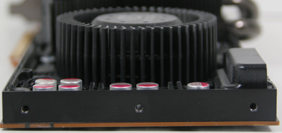
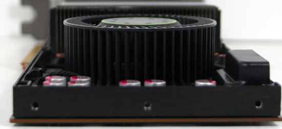
Finally, with average and maximum power consumption dealt with, NVIDIA turned to improving cooling on the GTX to bring temperatures down and to more quietly dissipate heat. GTX 480 not only was loud, but it had an unusual cooling design that while we’re fine with, ended up raising eyebrows elsewhere. Specifically NVIDIA had heatpipes sticking out of the GTX 480, an exposed metal grill over the heatsink, and holes in the PCB on the back side of the blower to allow it to breathe from both sides. Considering we were dissipating over 300W at times it was effective, but apparently not a design NVIDIA liked.
So for GTX 580 NVIDIA has done a lot of work under the hood to produce a card that looks less like the GTX 480 and more like the all-enclosed coolers we saw with the GTX 200 series; the grill, external heatpipes, and PCB ventilation holes are all gone from the GTX 580, and no one would hold it against you to mistake it for a GTX 285. The biggest change in making this possible is NVIDIA’s choice of heatsink: NVIDIA has ditched traditional heatpipes and gone to the new workhorse of vapor chamber cooling.
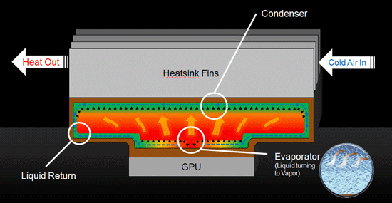
A Vapor Chamber Cooler In Action (Courtesy NVIDIA)
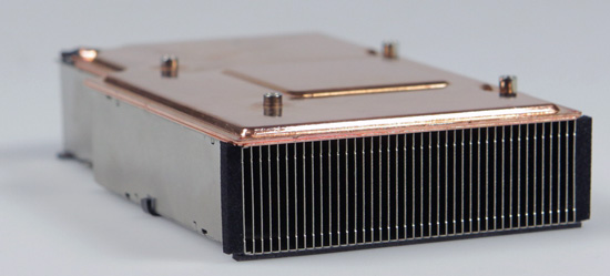
The GTX 580's Vapor Chamber + Heatsink
Vapor chamber coolers have been around for quite some time as aftermarket/custom coolers, and are often the signature design element for Sapphire; it was only more recently with the Radeon HD 5970 that we saw one become part of a reference GPU design. NVIDIA has gone down the same road and is now using a vapor chamber for the reference GTX 580 cooler. Visually this means the heatpipes are gone, while internally this should provide equal if not better heat conduction between the GPU’s heatspreader and the aluminum heatsink proper. The ultimate benefit from this being that with better heat transfer it’s not necessary to run the blower so hard to keep the heatsink cooler in order to maximize the temperature difference between the heatsink and GPU.
NVIDIA’s second change was to the blower itself, which is the source of all noise. NVIDIA found that the blower on the GTX 480 was vibrating against itself, producing additional noise and in particular the kind of high-pitch whining that makes a cooler come off as noisy. As a result NVIDIA has switched out the blower for a slightly different design that keeps a ring of plastic around the top, providing more stability. This isn’t a new design – it’s on all of our Radeon HD 5800 series cards – but much like the vapor chamber this is the first time we’ve seen it on an NVIDIA reference card.
Top: GTX 480 Blower. Bottom: GTX 580 Blower
Finally, NVIDIA has also tinkered with the shape of the shroud encasing the card for better airflow. NVIDIA already uses a slightly recessed shroud near the blower in order to allow some extra space between it and the next card, but they haven’t done anything with the overall shape until now. Starting with the GTX 580, the shroud is now slightly wedge-shaped between the blower and the back of the card; this according to NVIDIA improves airflow in SLI setups where there’s a case fan immediately behind the card by funneling more fresh air in to the gap between cards.


160 Comments
View All Comments
deeps6x - Tuesday, November 9, 2010 - link
Really, who has to have this card when for less money, you can get better results with a pair of 460s in SLI or a pair of 6850s in CF (even better than 460s in almost all cases) to give you better numbers than this card.Take the extra $100+ and bump your CPU up a speed bin or two.
Alberto8793 - Tuesday, November 9, 2010 - link
I will give Nvidia some props they have a very fast card, but interms of performance per dollar, AMD beats them out, go to newegg and click on the 5970 its 499$, go and check the 580, a cool 560$ now return to the anandtech review and check out the benchmarks, they speak for themselves, and finnally load and idle consumption of a two gpu card are lower than a single gpu?!?!?!?!? OUTRAGEOUS!slick121 - Wednesday, November 10, 2010 - link
I mean this is the "enough said!" post. So true, totally agree!ClagMaster - Tuesday, November 9, 2010 - link
Looks like Nvidia has done their homework optimize the GF100 after business pressures to release the GTX-480.Nvidia did a competent makeover of the GF100 and GTX-480 to reduce power, heat and noise.
The GF-110/GTX-580 offers about 10% more performance for the Watts, which are still too high. for my liking.
AnnonymousCoward - Wednesday, November 10, 2010 - link
I think it's more like 30% more performance per watt. Crysis power is 389W vs 421W and averages 15% more fps.the_elvino - Wednesday, November 10, 2010 - link
I would take Anand's power consumtion measurements of 421W for the GTX 480 and 389W for GTX 590 with a few pinches of salt.HardOCP compared the power draw in SLI and recorded following numbers for the entire system under full load:
GTX 480 SLI: 715W
GTX 590 SLI: 700W
Difference per card between 480 and 590: 7,5W!
The 590 is noticeably cooler though.
http://hardocp.com/article/2010/11/09/nvidia_gefor...
7Enigma - Wednesday, November 10, 2010 - link
Why would HardOCP's numbers be any more accurate than Anand's? One is comparing SLI and one is single card. We have no clue the differences in system configuration (individual variances of parts not the part name), not to mention the inherent variability of the cards themselves.I've said it in the 6850 article and before but power consumption numbers (and thus noise/heat) have to be taken with a grain of salt because there is no independent unbiased source giving these cards for review. A really good or poor cherry-picked sample can completely change the impression of a cards efficiency. And since we know NVIDIA ships cards with varying load voltages it is very easy to imagine a situation where one card would be similar in power draw to the 480 while another would show lower thermals.
Anand/Ryan I've said it before and I'll say it again, you have the chance to be a pioneer in the review field by getting independent sources of cards slightly after release. Yes your original review would have to exclude this (or have a caveat that this is what the manufacturer supplied you with).
Decide on a good number (3-5 shouldn't be unreasonable), and purchase these from etailers/locally anonymously. Test them for power/noise/temp and then either sell them on Ebay at slightly reduced cost or even increased price? (Anandtech approved!...touched by Ryan himself!....whatever....you've got a marketing department) :), and/or take one/all and give them away to your loyal readers like the other contests.
Then have a followup article with the comparisons between the "real" cards and the cherry-picked ones from NVIDIA/AMD. Just think how if the manufacturers know that you might call them out on a cherry-picked sample in a follow-up review, they might just try to avoid the bad press and ship one more closely in line with the product line.
Goblerone - Tuesday, November 9, 2010 - link
I'm confused here. In your review of ATI's new 6870, you were comparing against factory overclocked NVIDIA cards but here you are using reference ATI cards.What gives?
AnandThenMan - Wednesday, November 10, 2010 - link
Why even bother asking. It's clear that Anandtech is not about fairness in reviews anymore. Nvidia got special treatment, plain and simple.Just wait until we see Anandtech preview AMD's Brazos with some benches, you will see even more bizarre and head scratching benchmarks. Wait and see.
Sihastru - Wednesday, November 10, 2010 - link
Lol, give it a rest man... and while you're at it tells us about some similarly priced factory overclocked cards that AMD has on the stores shelves and could be used at the time the review was conducted. Relevent models only please, that have the same performance as the GTX580.