AMD's Radeon HD 6970 & Radeon HD 6950: Paving The Future For AMD
by Ryan Smith on December 15, 2010 12:01 AM ESTCayman: The Last 32nm Castaway
With the launch of the Barts GPU and the 6800 series, we touched on the fact that AMD was counting on the 32nm process to give them a half-node shrink to take them in to 2011. When TSMC fell behind schedule on the 40nm process, and then the 32nm process before canceling it outright, AMD had to start moving on plans for a new generation of 40nm products instead.
The 32nm predecessor of Barts was among the earlier projects to be sent to 40nm. This was due to the fact that before 32nm was even canceled, TSMC’s pricing was going to make 32nm more expensive per transistor than 40nm, a problem for a mid-range part where AMD has specific margins they’d like to hit. Had Barts been made on the 32nm process as projected, it would have been more expensive to make than on the 40nm process, even though the 32nm version would be smaller. Thus 32nm was uneconomical for gaming GPUs, and Barts was moved to the 40nm process.
Cayman on the other hand was going to be a high-end part. Certainly being uneconomical is undesirable, but high-end parts carry high margins, especially if they can be sold in the professional market as compute products (just ask NVIDIA). As such, while Barts went to 40nm, Cayman’s predecessor stayed on the 32nm process until the very end. The Cayman team did begin planning to move back to 40nm before TSMC officially canceled the 32nm process, but if AMD had a choice at the time they would have rather had Cayman on the 32nm process.
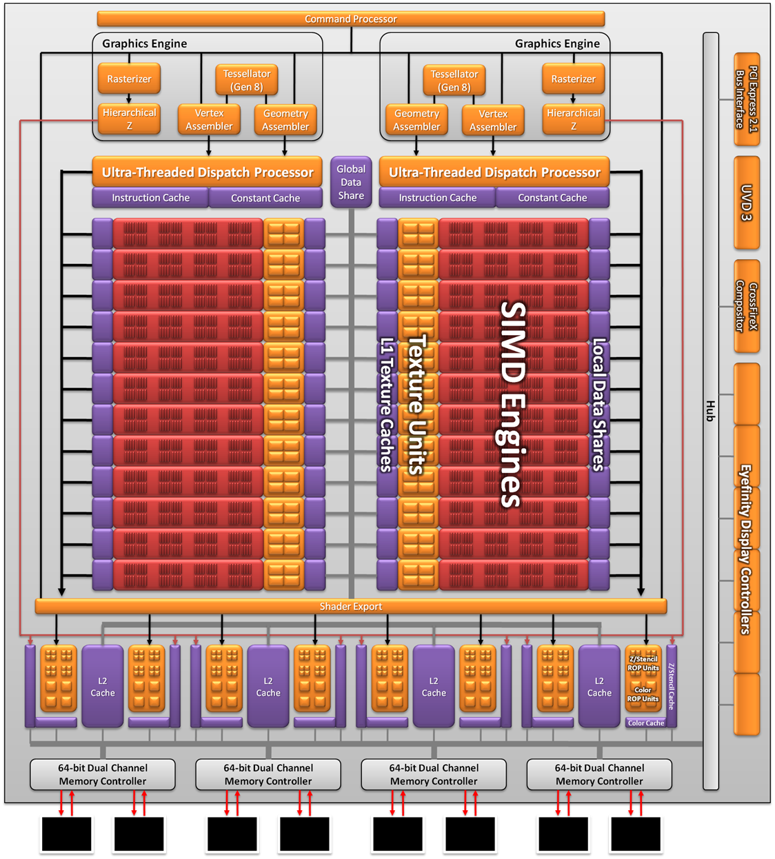
As a result the Cayman we’re seeing today is not what AMD originally envisioned as a 32nm part. AMD won’t tell us everything that they had to give up to create the 40nm Cayman (there has to be a few surprises for 28nm) but we do know a few things. First and foremost was size; AMD’s small die strategy is not dead, but getting the boot from the 32nm process does take the wind out of it. At 389mm2 Cayman is the largest AMD GPU since the disastrous R600, and well off the sub-300mm2 size that the small die strategy dictates. In terms of efficient usage of space though AMD is doing quite well; Cayman has 2.64 billion transistors, 500mil more than Cypress. AMD was able to pack 29% more transistors in only 16% more space.
Even then, just reaching that die size is a compromise between features and production costs. AMD didn’t simply settle for a larger GPU, but they had to give up some things to keep it from being even larger. SIMDs were on the chopping block; 32nm Cayman would have had more SIMDs for more performance. Features were also lost, and this is where AMD is keeping mum. We know PCI Express 3.0 functionality was scheduled for the 32nm part, where AMD had to give up their PCIe 3.0 controller for a smaller 2.1 controller to make up for their die size difference. This in all honesty may have worked out better for them: PCIe 3.0 ended up being delayed until November, so suitable motherboards are still at least months away.
The end result is that Cayman as we know it is a compromise to make it happen on 40nm. AMD got their new VLIW4 architecture, but they had to give up performance and an unknown number of features to get there. On the flip side this will make 28nm all the more interesting, as we’ll get to see many of the features that were supposed to make it for 2010 but never arrived.


168 Comments
View All Comments
cyrusfox - Wednesday, December 15, 2010 - link
You should totally be able to do a 4X1 display, 2 DP and 2 DVI, as long as one of those DP dells also has a DVI input. That would get rid of the need for your usb-vga adapter.gimmeagdlaugh - Wednesday, December 15, 2010 - link
Not sure why AMD 6970 has green bar,while NV 580 has red bar...?
medi01 - Wednesday, December 15, 2010 - link
Also wondering. Did nVidia marketing guys called again?Ryan Smith - Wednesday, December 15, 2010 - link
I normally use green for new products. That's all there is to it.JimmiG - Wednesday, December 15, 2010 - link
Still don't like the idea of Powertune. Games with a high power load are the ones that fully utilize many parts of the GPU at the same time, while less power hungry games only utilize parts of it. So technically, the specifications are *wrong* as printed in the table on page one.The 6970 does *not* have 1536 stream processors at 880 MHz. Sure, it may have 1536 stream processors, and it may run at up to 880 MHz.. But not at the same time!
So if you fully utilize all 1536 processors, maybe it's a 700 MHz GPU.. or to put it another way, if you want the GPU to run at 880 MHz, you may only utilize, say 1200 stream processors.
cyrusfox - Wednesday, December 15, 2010 - link
I think Anand did a pretty good job of explaining at how it reasonably power throttles the card. Also as 3rd party board vendors will probably make work-arounds for people who abhor getting anything but the best performance(even at the cost of efficiency). I really don't think this is much of an issue, but a good development that is probably being driven by Fusion for Ontario, Zacate, and llano. Also only Metro 2033 triggered any reduction(850Mhz from 880Mhz). So your statement of a crippled GPU only holds for Furmark, nothing got handicapped to 700Mhz. Games are trying to efficiently use all the GPU has to offer, so I don't believe we will see many games at all trigger the use of powertune throttling.JimmiG - Wednesday, December 15, 2010 - link
Perhaps, but there's no telling what kind of load future DX11 games, combined with faster CPUs will put on the GPU. Programs like Furmark don't do anything unusual, they don't increase GPU clocks or voltages or anything like that - they just tell the GPU - "Draw this on the screen as fast as you can".It's the same dilemma overclockers face - Do I keep this higher overclock that causes the system to crash with stress tests but works fine with games and benchmarks? Or do I back down a few steps to guarantee 100% stability. IMO, no overclock is valid unless the system can last through the most rigorous stress tests without crashes, errors or thermal protection kicking in.
Also, having a card that throttles with games available today tells me that it's running way to close to the thermal limit. Overclocking in this case would have to be defined as simply disabling the protection to make the GPU always work at the advertised speed.
It's a lazy solution, what they should have done is go back to the drawing board until the GPU hits the desired performance target while staying within the thermal envelope. Prescott showed that you can't just keep adding stuff without any considerations for thermals or power usage.
AnnihilatorX - Wednesday, December 15, 2010 - link
Didn't you see you can increase the throttle threshold by 20% in Catalyst Control Centre. This means 300W until it throttles, which in a sense disables the PowerTune.Mr Perfect - Thursday, December 16, 2010 - link
On page eight Ryan mentions that Metro 2033 DID get throttled to 700MHz. The 850MHz number was reached by averaging the amount of time Metro was at 880MHz with the time it ran at 700MHz.Which is a prime example of why I hate averages in reviews. If you have a significantly better "best case", you can get away with a particularly bad "worst case" and end up smelling like roses.
fausto412 - Wednesday, December 15, 2010 - link
CPU's have been doing this for a while...and you are allowed to turn the feature off. AMD is giving you a range to go over.It will cut down on RMA's, Extend Reliability.