The Intel SSD 710 (200GB) Review
by Anand Lal Shimpi on September 30, 2011 8:53 PM EST- Posted in
- Storage
- SSDs
- Intel
- Intel SSD 710
NAND Recap
Flash memory is non-volatile storage and in that sense it's similar to a hard drive. Once you write to a NAND flash cell it can store that data for an extended period of time without power.
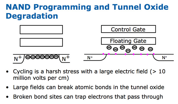
You write to NAND through a quantum tunneling process. Apply a high enough voltage across a floating-gate transistor and some electrons will actually tunnel through an insulating oxide layer and remain on the floating gate, even when the voltage is removed. Repeated tunneling can weaken the bonds of the oxide, eventually allowing electrons to freely leave the floating gate. It's this weakening that's responsible for a lot of NAND endurance issues, although there are other elements at play.
NAND is programmed and read by seeing how each cell responds to various voltages. This chart shows the difference between MLC (multi-level-cell) and SLC (single-level-cell) NAND:
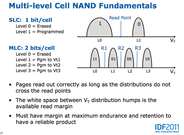
Both types of NAND are identical architecturally, it's just a question of how many voltages you map to bits on the cell. MLC (2-bit-per-cell ) has four different voltage levels that correspond to values while SLC only has two. Note that each value can correspond to a distribution of voltages. As long as the threshold voltage falls within that range, the corresponding value is programmed or read.
The white space in between each voltage distribution is the margin you have to work with. Those blue lines above are read points. As long as the voltage distributions don't cross the read points, data is accessed correctly. The bigger the margin between these points, the more write cycles you'll get out of your NAND. The smaller the margin, the easier it is to produce the NAND. It's easier to manufacture NAND that doesn't require such precise voltages to store and read data from each cell. Over time physical effects can cause these voltage distributions to shift, which ultimately leads to cell failure.
As MLC NAND gets close to the end of its life, these margins start narrowing considerably. Continuously programming and erasing NAND cells weakens the oxide, eventually allowing electrons to become stuck in the oxide itself. This phenomenon alters the threshold voltage of the transistor, which in turn shifts bit placements:
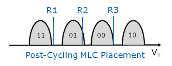
There's now ambiguity between bits which, if this cell were allowed to remain active in an SSD, would mean that when you go to read a file on your drive there's a chance that you won't actually get the data you're requesting. A good SSD should mark these bits bad at this point.
There's a JEDEC spec that defines what should happen to the NAND once its cells get to this point. For consumer applications, the NAND should remain in a read-only state that can guarantee data availability for 12 months at 30C with the drive powered off. Manufacturers must take this into account when they test and qualify their NAND. If you're curious, JEDEC also offers guidelines on how to cycle test the NAND to verify that it's compliant.
By now we all know the numbers. At 50nm Intel's MLC NAND was rated for 10,000 program/erase cycles per cell. That number dropped to 5,000 at 34nm and remained at the same level with the move to 25nm. Across the industry 3,000 - 5,000 p/e cycles for 2x-nm 2-bit-per-cell MLC (2bpc) NAND is pretty common.
For desktop workloads, even the lower end of that range is totally fine. The SSD in your desktop or notebook is more likely to die because of some silly firmware bug or manufacturing issue than you wearing out the NAND. For servers with tons of random writes, even 5K p/e cycles isn't enough. To meet the needs of these applications, Intel outfitted the 710 with MLC-HET (High Endurance Technology) more commonly known as eMLC.
Fundamentally, Intel's MLC-HET is just binned MLC NAND. SLC NAND gets away with having ultra high p/e cycle counts by only having two bit levels to worry about. The voltage distributions for those two levels can be very far apart and remain well defined over time as a result. I suspect only the highest quality NAND was used as SLC to begin with, also contributing to its excellent endurance.
Intel takes a similar approach with MLC-HET. Placements are much more strict in MLC-HET. Remember what I said earlier, narrow ranges of voltages mapping to each bit level reduces the number of NAND die that will qualify, but you build in more margin as you cycle the NAND. If placements do shift however, Intel's SSD 710 can actually shift read points as long as the placements aren't overlapping.
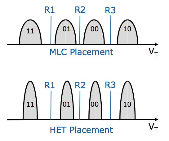
Similar to frequency binning CPUs, the highest quality NAND with the tightest margins gets binned into MLC-HET while everything else is shipped as standard MLC. And just like with frequency binning, there's a good chance you'll get standard MLC that will last a lot longer than it's supposed to. In fact, I've often heard from manufacturers that hitting up to 30K p/e cycles on standard MLC NAND isn't unrealistic. With its MLC-HET Intel also more frequently/thoroughly refreshes idle NAND cells to ensure data integrity over periods of extended use.
Intel performs one other optimization on MLC-HET. After you've exceeded all available p/e cycles on standard MLC, JEDEC requires that the NAND retain your data in a power-off state for a minimum of 12 months. For MLC-HET, the minimum is reduced to 3 months. In the consumer space you need that time to presumably transfer your data over. In the enterprise world, a dying drive is useless and the data is likely mirrored elsewhere. Apparently this tradeoff also helps Intel guarantee more cycles during the drive's useful life.
At IDF Intel told us the MLC-HET in the SSD 710 would be good for around 30x the write cycles of standard (presumably 25nm) MLC. If we use 3,000 as a base for MLC, that works out to be 90K p/e cycles for Intel's 25nm MLC-HET.


68 Comments
View All Comments
AnnonymousCoward - Sunday, October 2, 2011 - link
Use a CD; that's mechanical storage.Flash is definitely a poor choice, since charge is slowly lost. I'm not sure about magnetic hard drives.
ggathagan - Monday, October 3, 2011 - link
If you use optical media, better have it a manufactured ROM disk, as opposed to writable media.Even the best consumer optical media is only good for around 10 years.
James5mith - Monday, October 3, 2011 - link
One thing intel and the rest of the SSD crowd by far have failed to address is the limitations of SATA for enterprise workloads. Doesn't matter how fast your drive is, on a SATA interface it will tank in truly heavy mixed I/O environments. Native SAS SSD's are needed to move the hdd form factor SSD's forward in the industry.That being said, in my research for an in-house project, I discovered Smart Modular. Their Optimus SAS SSD's are up to 1.6TB/drive, and at that capacity are still below $3/GB.
To be fair, I have not gotten any of them in house to test yet, so I can't say how well they will do. But knowing the difference moving from SATA to SAS drives make in an array, I would have to imagine it will be significant when I do.
Not to mention, from a pure density standpoint, 1.6TB 2.5" SSDs can pack more density per rack unit than 3TB 3.5" drives. Once you get to the 4TB 3.5" drives, the crown returns to slow spinning media though.
jhh - Monday, October 3, 2011 - link
A conventional HDD wouldn't fare much better. The typical service life of an enterprise HDD is 5 years after a storage period of no more than 6 months. Beyond that point, the MTBF numbers aren't valid. That doesn't mean the drive will immediately fail. But, conventional HDDs aren't meant to be stored for a long period of time. The lubricating medium (grease or oil) will start moving away from where it is supposed to be, so that parts which were supposed to be lubricated won't be lubricated. The lubricant may also start oxidizing, becoming less of a lubricant. I'm not sure that a drive sitting around for 5 years will be any worse than a drive which was operating for 5 years, but I wouldn't count on either to be around for 20 years, let alone 50.If you want to be sure those baby pictures will still be around to show their grandkids, best to print the pictures, as we have never developed a better archival storage device. Better yet, paint it in some obscure cave in France. If you want the time capsule information to be available, print it on archival paper with archival inks.
rikmorgan - Tuesday, October 11, 2011 - link
I see an article in EE Times saying Samsung is producing flash NAND on their new 20nm FAB now and expects to begin running it at 10nm next year. Just passing it on, don't know how newsworthy it is. ET Times 10/10/2011 edition.Linkpl4y - Saturday, October 15, 2011 - link
Well you've made it this far. Hopefully you've learned something on the way.Here's the next path on your journey. http://bit.ly/nqPUwd
Iketh - Monday, October 17, 2011 - link
LOLmayaw - Saturday, November 5, 2011 - link
Because I do video graphics and its really the only thing that slows my system down for any type of reference # on tests. Even with a 10,000 RPM drive I have 12gb of mem and I upgrade my processor every 3-4 years when I can but I really never think of the hard drive. But now I am seriously thinking about getting one of these.Oh and by the way guys I think that the collar of his shirt is stretched out because his head is so big and it has to stretch itself out cause of the big brain he has in it unlike ppl who are arguing about someone that is wearing a t-shirt on a hard drive review.