Gigabyte GA-7PESH1 Review: A Dual Processor Motherboard through a Scientist’s Eyes
by Ian Cutress on January 5, 2013 10:00 AM EST- Posted in
- Motherboards
- Gigabyte
- C602
Visual Inspection
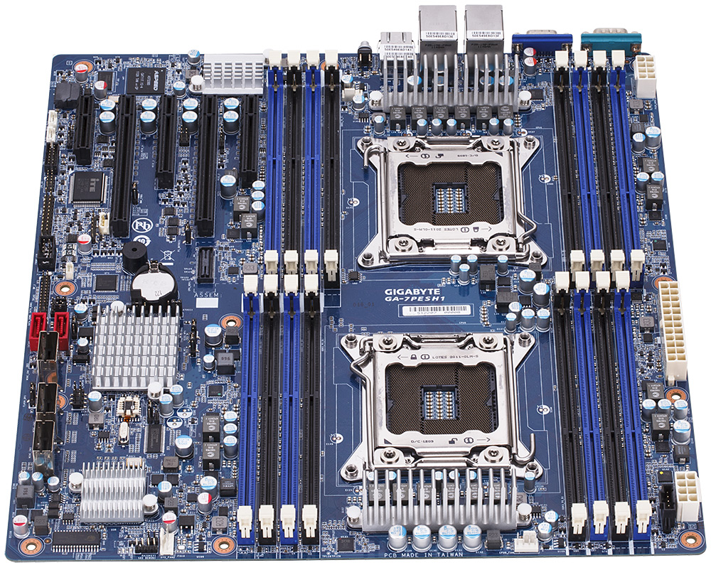
I knew server boards were large, but coming from the ATX and E-ATX standards, this thing is huge. It measures 330mm x 305mm (13” x 12”) which correlates to the SSI EEB specification for server motherboards. This is the size exact size of an official E-ATX motherboard (despite a small amount of loose definition), but to put the icing on the cake, the mounting holes for the motherboard are different to the normal ATX standards. If we took a large case, like the Rosewill Blackhawk-Ultra, it supports ATX, SSI CEB, XL-ATX, E-ATX and HPTX, up to 13.6” x 15”, but not SSI EEB. Thus drilling extra holes for standoffs may be required.
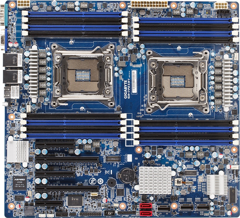
Unlike the SR-X or Z9PE-D8 WS, the GA-7PESH1 supports two memory modules per channel for all channels on board. In terms of specifications this means support for up to 128 GB UDIMM (i.e. regular DDR3), 128 GB UDIMM ECC, and 512 GB RDIMM ECC. Due to the nature of the design, only 1066-1600 MHz is supported, but the GA-7PESH1 supports 1600 MHz when all slots are populated. For our testing, Kingston has kindly supplied us with 8x4GB of their 1600 C11 ECC memory.
As with the majority of server boards, stability and longevity is a top priority. This means no overclocking, and Gigabyte can safely place a six phase power delivery on each CPU – it also helps that all SB-E Xeons are multiplier locked and there is no word of unlocked CPUs being released any time soon. As we look at the board, standards dictate that the CPU on the right is designated as the first CPU. Each CPU has access to a single fan header, and specifications for coolers are fairly loose in both the x and the y directions, limited only by memory population and the max z-height of the case or chassis the board is being placed into. As with all dual CPU motherboards, each CPU needs its own Power Connector, and we find them at the top of the board behind the memory slots and at opposite ends. The placement of these power connectors is actually quite far away for a normal motherboard, but it seems that the priority of the placement is at the edge of the board. In between the two CPU power connectors is a standard 24-pin ATX power connector.
One of the main differences I note coming from a consumer motherboard orientation is the sheer number of available connectors and headers on such a server motherboard. For example, the SATA ports have to be enabled by moving the jumpers the other side of the chipset. The chipset heatsink is small and basic – there is no need for a large heatsink as the general placement for such a board would be in a server environment where noise is not particularly an issue if there are plenty of Delta fans to help airflow.
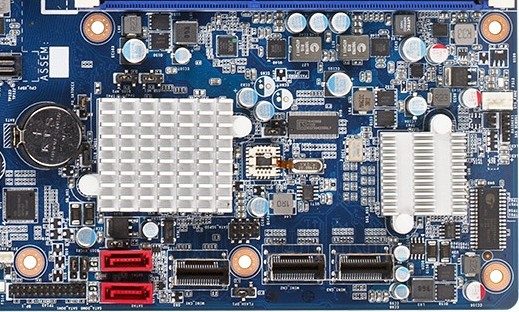
On the bottom right of the board we get a pair of SATA ports and three mini-SAS connections. These are all perpendicular to the board, but are actually in the way of a second GPU being installed in a ‘normal’ motherboard way. Users wishing to use the second PCIe x8 slot on board may look into PCIe risers to avoid this situation. The heatsink on the right of this image covers up an LSI RAID chip, allowing the mSAS drives to be hardware RAIDed.
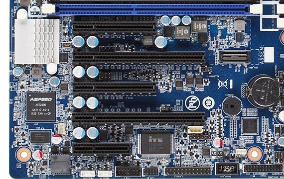
As per normal operation on a C602 DP board, the PCIe slots are taken from the PEG of one CPU. On some other boards, it is possible to interweave all the PCIe lanes from both CPUs, but it becomes difficult when organizing communication between the GPUs on different CPUs. From top to bottom we get an x8 (@x4), x16, x8 (@x4), x16 (@x8), x4(@x1). It seems odd to offer these longer slots at lower speed ratings, but all of the slots are Gen 3.0 capable except the x4(@x1). The lanes may have been held back to maintain data coherency.
To those unfamiliar with server boards, of note is the connector just to the right of center of the picture above. This is the equivalent of the front panel connection on an ATX motherboard. At almost double the width it has a lot more options, and where to put your cables is not printed on the PCB – like in the old days we get the manual out to see what is what.
On the far left we have an ASPEED AST2300 chip, which has multiple functions. On one hand it is an onboard 2D graphics chip which powers the VGA port via its ARM926EJ (ARM9) core at 400 MHz. For the other, it as an advanced PCIe graphics and remote management processor, supporting dual NICs, two COM ports, monitoring functions and embedded memory. Further round this section gives us a removable BIOS chip, a COM header, diagnostic headers for internal functions, and a USB 2.0 header.
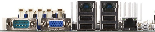
The rear IO is very bare compared to what we are normally used to. From left to right is a serial port, the VGA port, two gigabit Ethernet NICs (Intel I350), four USB 2.0 ports, the KVM server management port, and an ID Switch button for unit identification. There is no audio here, no power/reset buttons, and no two-digit debug LED. It made for some rather entertaining/hair removing scenarios when things did not go smoothly during testing.
Board Features
| Gigabyte GA-7PESH1 | |
| Price |
Contact: 17358 Railroad St. City of Industry CA 91748 +1-626-854-9338 |
| Size | SSI EEB |
| CPU Interface | LGA 2011 |
| Chipset | Intel C602 |
| Memory Slots |
Sixteen DDR3 DIMM slots supporting: 128GB (UDIMM) @ 1.5V 512GB (RDIMM) @ 1.5V 128GB DDR3L @ 1.35 V Quad Channel Arcitecture ECC RDIMM for 800-1600 MHz Non-ECC UDIMM for 800-1600 MHz |
| Video Outputs | VGA via ASPEED 2300 |
| Onboard LAN | 2 x Intel I350 supporting uo to 1000 Mbps |
| Onboard Audio | None |
| Expansion Slots |
1 x PCIe 3.0 x16 1 x PCIe 3.0 x16 (@ x8) 2 x PCIe 3.0 x8 (@ x4) 1 x PCIe 2.0 x4 (@ x1) |
| Onboard SATA/RAID |
2 x SATA 6 Gbps, Supporting RAID 0,1 2 x mini-SAS 6 Gbps, Supporting RAID 0,1 1 x mini-SAS 3 Gbps, Supporting RAID 0,1 |
| USB | 6 x USB 2.0 (Chipset) [4 back panel, 2 onboard] |
| Onboard |
2 x SATA 6 Gbps 2 x mSAS 6 Gbps 1 x mSAS 3 Gbps 1 x USB 2.0 Header 4 x Fan Headers 1 x PSMI header 1 x TPM header 1 x SKU KEY header |
| Power Connectors |
1 x 24-pin ATX Power Connector 2 x 8-pin CPU Power Connector |
| Fan Headers |
2 x CPU (4-pin) 2 x SYS (4-pin, 3-pin) |
| IO Panel |
1 x Serial Port 1 x VGA 2 x Intel I350 NIC 4 x USB 2.0 1 x KVM NIC 1 x ID Switch |
| Warranty Period | Refer to Sales |
| Product Page | Link |
Without having a direct competitor to this board on hand there is little we can compare such a motherboard to. In this level having server grade Intel NICs should be standard, and this board can take 8GB non-ECC memory sticks or 32GB ECC memory sticks, for a maximum of 512 GB. If your matrix solvers are yearning for memory, then this motherboard can support it.


64 Comments
View All Comments
mayankleoboy1 - Saturday, January 5, 2013 - link
Ian :How much difference do you think Xeon Phi will make in these very different type of Computations?
Will buying a Xeon Phi "pay itself out" as you said in the above comments ? (or is xeon phi linux only ?)
IanCutress - Saturday, January 5, 2013 - link
As far as we know, Xeon Phi will be released for Linux only to begin with. I have friends who have been able to play with them so far, and getting 700 GFlops+ in DGEMM in double precision.It always comes down to the algorithm with these codes. It seems that if you have single precision code that doesn't mind being in a 2P system, then the GPU route may be preferable. If not, then Phi is an option. I'm hoping to get my hands on one inside H1 this year. I just have to get my hands dirty with Linux as well.
In terms of the codes used here, if I were to guess, the Implicit Finite Difference would probably benefit a lot from Xeon Phi if it works the way I hope it does.
Ian
mayankleoboy1 - Saturday, January 5, 2013 - link
Rather stupid question, but have you tried using PGO builds ?Also, do you build the code with the default optimizations, or use the MSVC equivalent switch of -O2 ?
IanCutress - Saturday, January 5, 2013 - link
Using Visual Studio 2012, all the speed optimisations were enabled including /GL, /O2, /Ot and /fp:fast. For each part I analysed the sections which took the most time using the Performance Analysis tools, and tried to avoid the long memory reads. Hence the Ex-FD uses an iterative loading which actually boosts speed by a good 20-30% than without it.Ian
Klimax - Sunday, January 6, 2013 - link
Interesting. Why not Ox (all optimisations on)BTW: Do you have access to VTune?
IanCutress - Wednesday, January 9, 2013 - link
In case /Ox performs an optimisation for memory over speed in an attempt to balance optimisations. As speed is priority #1, it made more sense to me to optimise for that only. If VS2012 gave more options, I'd adjust accordingly.Never heard of VTune, but I did use the Performance Analysis tools in VS2012 to optimise certain parts of the code.
Ian
Beenthere - Saturday, January 5, 2013 - link
Business and mobo makers do not use 2P mobos to get high benches or performance bragging rights per se. These systems are build for bullet-proof reliability and up time. It does no good for a mobo/system to be 3% faster if it crashes while running a month long analysis. These 2P mobos are about 100% reliability, something rarely found in a enthusiasts mobo.Enterprise mobos are rarely sold by enthusiast marketeers. Newegg has a few enterprise mobos listed primarily because they have started a Newegg Biz website to expand their revenue streams. They don't have much in the line of true enterprise hardware however. It's a token offering because manufacturers are not likely to support whoring of the enterprise market lest they lose all of their quality vendors who provide customer technical product support.
psyq321 - Sunday, January 6, 2013 - link
Actually, ASUS Z9PE-D8 WS allows for some overclocking capabilities.CPU overclocking with 2P/4P Xeon E5 (2600/4600 sequence) is a no-go because Intel explicitly did not store proper ICC data so it is impossible to manipulate BCLK meaningfully (set the different ratios). Oh, and the multipliers are locked :)
However, Z9PE D8 WS allows memory overclocking - I managed to run 100% 24/7 stable with the Samsung ECC 1600 DDR3 "low voltage" RAM (16 GB sticks) - just switching memory voltage from 1.35v to 1.55v allows overclocking memory from 1600 MHz to 2133 MHz.
Why would anyone want to do that in a scientific or b2b environment? The only usage I can see are applications where memory I/O is the biggest bottleneck. Large-scale neural simulations are one of such applications, and getting 10 GB/s more of memory I/O can help a lot - especially if stable.
Also, low-latency trading applications are known to benefit from overclocked hardware and it is, in fact, used in production environment.
Modern hardware does tend to have larger headrooms between the manufacturer's operating point and the limits - if the benefit from an overclock is more benefitial than work invested to find the point where the results become unstable - and, of course, shorter life span of the hardware - then, it can be used. And it is used, for example in some trading scenarios.
Drazick - Saturday, January 5, 2013 - link
Will You, Please, Update Your Google+ Page?It would be much easier to follow you there.
Ryan Smith - Saturday, January 5, 2013 - link
Our Google+ page is just a token page. If you wish to follow us then your best option is to follow our RSS feeds.