The ARM Diaries, Part 2: Understanding the Cortex A12
by Anand Lal Shimpi on July 17, 2013 12:30 PM EST- Posted in
- CPUs
- Arm
- SoCs
- Cortex A12
A couple of weeks ago I began this series on ARM with a discussion of the company’s unique business model. In covering semiconductor companies we’ve come across many that are fabless, but it’s very rare that you come across a successful semiconductor company that doesn’t even sell a chip. ARM’s business entirely revolves around licensing IP for its instruction set as well as its own CPU (and now GPU and video) cores.
Before we get into discussions of specific cores, it’s important to talk about ARM’s portfolio as a whole. In the PC space we’re used to focusing on Intel’s latest and greatest microarchitectures, which are then scaled in various ways to hit lower price targets. We might see different core counts, cache sizes, frequencies and maybe even some unfortunate instruction set tweaking but for the most part Intel will deliver a single microarchitecture to cover the vast majority of the market. These days, this microarchitecture is simply known as Core.
Back in 2008, Intel introduced a second microarchitecture under the Atom brand to target lower cost (and lower power) markets. The combination of Atom and Core spans the overwhelming majority of the client computing market for Intel. The prices of these CPUs range from the low double digits with Atom to many hundreds of dollars for the highest end Core processors (the most expensive desktop Haswell is $350, however mobile now extends up to $1100). There are other designs that target servers (which are then repurposed for ultra high-end desktops), but those are beyond the scope of this discussion for now.
If we limit our discussion to personal computing devices (smartphones, tablets, laptops and desktops), where Intel uses two microarchitectures ARM uses three. The graphic below illustrates the roadmap:
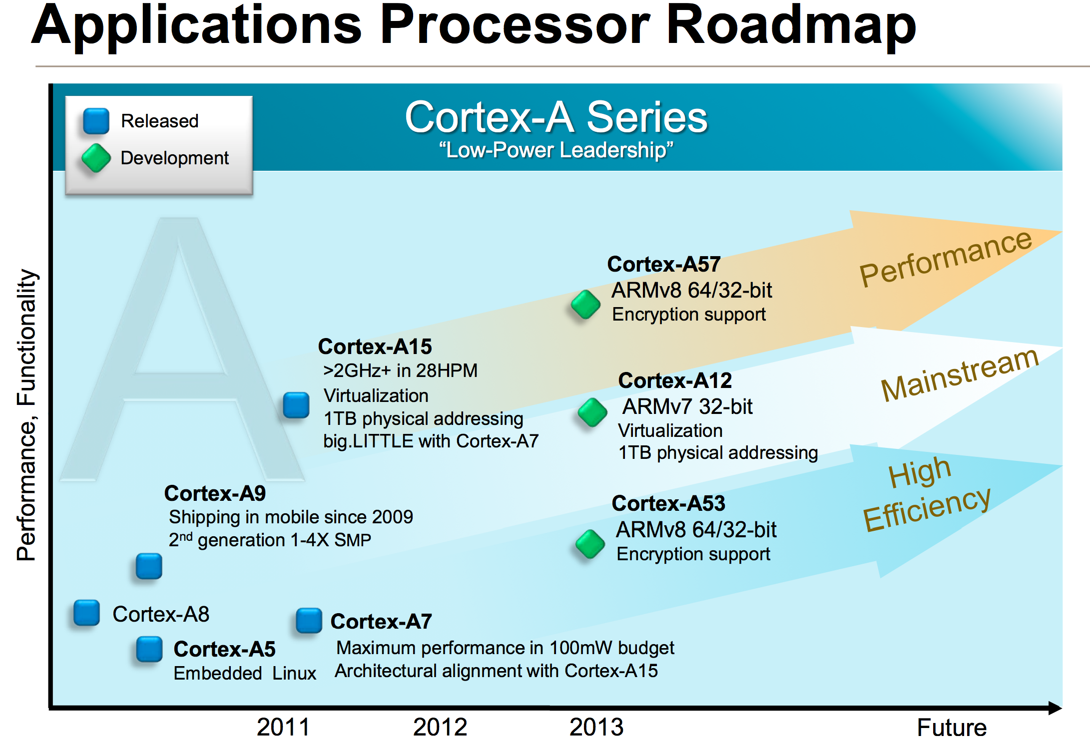
You need to somewhat ignore the timescale on the x-axis since those dates really refer to when ARM IP is first available to licensees, not when products are shipping to consumers, but you get an idea for the three basic vectors of ARM’s Cortex A-series of processor IP. Note that there are also Cortex R (embedded) and Cortex M (microcontroller) series of processor IP offered as well, but once again those are beyond the scope of our discussion here.
If we look at currently available cores, there’s the Cortex A15 on the high end, Cortex A9 for the mainstream and Cortex A7 for entry/low cost markets. If we’re to draw parallels with Intel’s product lineup, the Cortex A15 is best aligned with ultra low power/low frequency Core parts (think Y-series SKUs), while the Cortex A9 vector parallels Atom. Cortex A7 on the other hand targets a core size/cost/power level that Intel doesn’t presently address. It’s this third category labeled high efficiency above that Intel doesn’t have a solution for. This answers the question of why ARM needs three microarchitectures while Intel only needs two: in mobile, ARM targets a broader spectrum of markets than Intel.
Dynamic Range
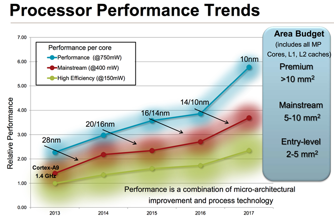
If you’ve read any of our smartphone/tablet SoC coverage over the past couple of years you’ll note that I’m always talking about an increasing dynamic range of power consumption in high-end smartphones and tablets. Each generation performance goes up, and with it typically comes a higher peak power consumption. Efficiency improvements (either through architecture, process technology or both) can make average power in a reasonable workload look better, but at full tilt we’ve been steadily marching towards higher peak power consumption regardless of SoC vendor. ARM provided a decent overview of the CPU power/area budget as well as expected performance over time of its CPU architectures:

Looking at the performance segment alone, we’ll quickly end up with microarchitectures that are no longer suited for mobile, either because they’re too big/costly or they draw too much power (or both).
The performance vector of ARM CPU IP exists because ARM has its sights set higher than conventional smartphones. Starting with the Cortex A57, ARM hopes to have a real chance in servers (and potentially even higher performance PCs, Windows RT and Chrome OS being obvious targets).
Although we see limited use of ARM’s Cortex A15 in smartphones today (some international versions of the Galaxy S 4), it’s very clear that for most phones a different point on the power/performance curve makes the most sense.
The Cortex A8 and A9 were really the ARM microarchitectures that drove smartphone performance over the past couple of years. The problem is that while ARM’s attentions shifted higher up the computing chain with Cortex A15, there was no successor to take the A9’s place. ARM’s counterpoint would be that Cortex A15 can be made suitable for lower power operation, however its partners (at least to date) seemed to be focused on extracting peak performance from the A15 rather than pursuing a conservative implementation designed for lower power operation. In many ways this makes sense. If you’re an SoC vendor that’s paying a premium for a large die CPU, you’re going to want to get the most performance possible out of the design. Only Apple seems to have embraced the idea of using die area to deliver lower power consumption.
The result of all of this is that the Cortex A9 needed a successor. For a while we’d been hearing about a new ARM architecture that would be faster than Cortex A9, but lower power (and lower performance) than Cortex A15. Presently, the only architecture in between comes from Qualcomm in the form of some Krait derivative. For ARM to not let its IP licensees down, it too needed a solution for the future of the mainstream smartphone market. Last month we were introduced to that very product: ARM’s Cortex A12.
Slotting in numerically between A9 and A15, the initial disclosure unfortunately didn’t come with a whole lot of actual information. Thankfully, we now have some color to add.


65 Comments
View All Comments
lmcd - Wednesday, July 17, 2013 - link
Where do various Kraits fit in?Wilco1 - Wednesday, July 17, 2013 - link
The Krait 800 as used in Galaxy S4 fits between A9 and A9R4 (it is ~5% better IPC than A9 - it makes up for that by clocking very high).tuxRoller - Wednesday, July 17, 2013 - link
Can you provide a reference for these values?The geekbench numbers are all over the place even for the same device (for instance, you see iphone 5 results that vary by 6%, while gs4 can vary by 16% easily).
Death666Angel - Thursday, July 18, 2013 - link
Not sure what geekbench measures and saves. But considering the multitude of options for tweaking an Android system is quite easy. Just change a some governors around and use a different scheduler and you can get quite the range of results.tuxRoller - Sunday, July 21, 2013 - link
That's kinda my point.Where exactly is he getting his numbers from.
michael2k - Wednesday, July 17, 2013 - link
It really does sound like the Swift or Krait cores, but widely available now to the Rockchips and Mediateks. Even if it comes out next year, it means $200 smartphones with the raw performance of an iPhone 5 or Galaxy S4 while Apple and Samsung sell something similar for $450. The real question then is how Qualcomm, Samsung, and Apple will push their architectures other than more die-shrinks. Apple still has the option of moving to 4 core as well as BIG.little, and Qualcomm still has the option of BIG.little as well, but where is Exynos going to head? 8 core BIG.little (for 16 total cores?) Asymmetric B.l with 8 big cores and 4 small cores? Something else altogether?fteoath64 - Friday, July 19, 2013 - link
Great point regarding Big.Little design in the SoC. There are many ways to implement Big.Little design on the wafer. I think only the rudimentary one has been used and this does not really link as much to OS optimizations as we would like. It takes effort/complexity and great code in drivers and kernel changes to take advantage of the design in order to maximise what the hardware can do. And there is the variant that could go Big.Medium.Little. If you look at the frequency charts of typical use, the Medium state do take a lot of the time duration while the Big takes very little (only in the spikes) then the Little takes care of near idle time. Having a Medium module takes space but might be worth the effort in power savings more than just Big.Little switching. The switching cost in power is negligible but time sustained power use on a certain frequency do have good savings (eg 30% in Medium state vs 5% on Big state). Optimizing the OS to change state is important as the efficiency and time savings are there to be had. The slower it does it, the more power it draws for a given duration. Another software optimizing is to split threads to specific core types or core number to optimise performance. eg Little core does all I/O since that is slow while FP/INT goes to Big, or INT split between Big and Little. Dynamic switching to keep one Big core active for several seconds longer might be a benefit if it gets triggered soon after, ie Why switch when a delay in switch solves the problem!. OF course a huge simulation is needed to find the optimal design points that are worth implementing. It is an iterative process. The same goes for GPU cores to get active and boost frequency on demand. For now, they kick fully blast when the game wants it. A great feedback way would be an FPS counter to throttle down the gpus since > 60fps is pretty useless unless you are running 120fps 3D displays. For that cap it at 120fps when the is mode is used. Due to the time to release durations, I am certain many compromised were made just to get the silicon out. ARM vendors are not like Intel who can afford the wait on a release because they had a monopoly on the chip in the market. Competition ensure that ARM evolves quickly and efficiently. This is where you can see Qualcomm succeeding while Tegra falters. Samsung is trying to find their secret sauce toward success with Octa-core design. I think next iteration might be a good one for them coupled with process node improvements they will use.I see a 2:3:4 design as optimum. 2Big 3Medium 4 Little. Here is how it should work:
Full Bore: 2Big 2Medium and 1 Little active (PentaCore design).
Medium operation: 3Medium and 2 Little active (Still holding PentaCore threading)
Step Down1: 1Medium 2 Little.
Idle: 1 Little only. Note Little takes ALL the I/O traffic.
roberto.tomas - Wednesday, July 17, 2013 - link
Looks pretty clear to me that there will be an A55 at 14nm or at least 10nm. The A12 is technically replacing the A9, right at the start of the next gen of chips which are all 64 bit. It doesn't do them any good to have a high end and low end chip that is 64 bit, and a mid range chip that is only 32 bit. But the power/performance claims are very close to the A15... so this is basically replacing the A15, from that perspective.The A57 will expire sometime at/after 14nm, and new designs will come out. At that time, an A55 that replaces it would make sense, fulfilling the same roll as the A12 at 32-bit.
Qwertilot - Wednesday, July 17, 2013 - link
I'm sure I remember reading somewhere (some interview?) that they decided that it just didn't make sense (yet) to go 64 bit for the sorts of devices that the A12 will be targeting. The A57 obviously has to go 64 bit to support servers and the like, and that presumably means that the A53 has to follow in order to be matched for bigLittle purposes for high end smart phones/tablets etc.As michael2k refers to above, the A12 is aimed more at mid/in time, low end phones and the like. Much less reason to push 64 bit there just yet. ARM have to support this sort of thing but I guess the business model means that they can too.
WhitneyLand - Wednesday, July 17, 2013 - link
The NEON improvements are compelling, but it would be nice to peek behind the curtain of the 48% improvement claims on FFMPEG.To start FFMPEG covers a vast amount of functionality, but certain FFMPEG codecs like h.264 are much more relevant than the obscure ones. So which codecs were used, and are the improvements seen in encoding or decoding, or both?
As we learned with AVX and x264, it's not always easy to realize big gains in real life scenarios with new SIMD hardware.
If there's interest in an article benchmarking x264 on the A9/A15/Krait (to tide us over until the A12 arrives) let me know, been trying to find a way to contribute to AT. :)