AMD Kaveri Review: A8-7600 and A10-7850K Tested
by Ian Cutress & Rahul Garg on January 14, 2014 8:00 AM ESTLlano, Trinity and Kaveri Die: Compared
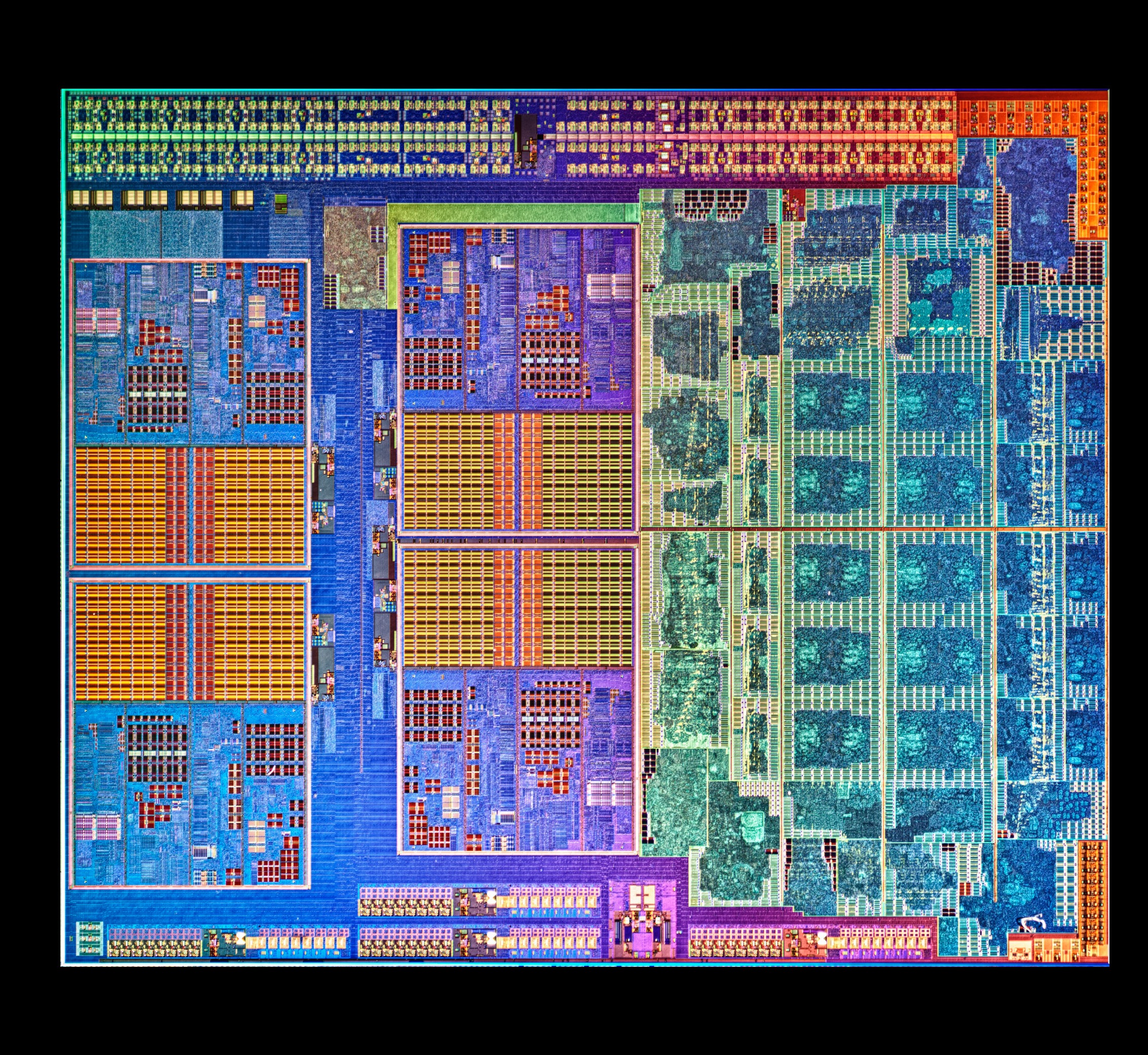
AMD sent along a high res shot of Kaveri's die. Armed with the same from the previous two generations, we can get a decent idea of the progression of AMD's APUs:
Llano, K10 Quad Core

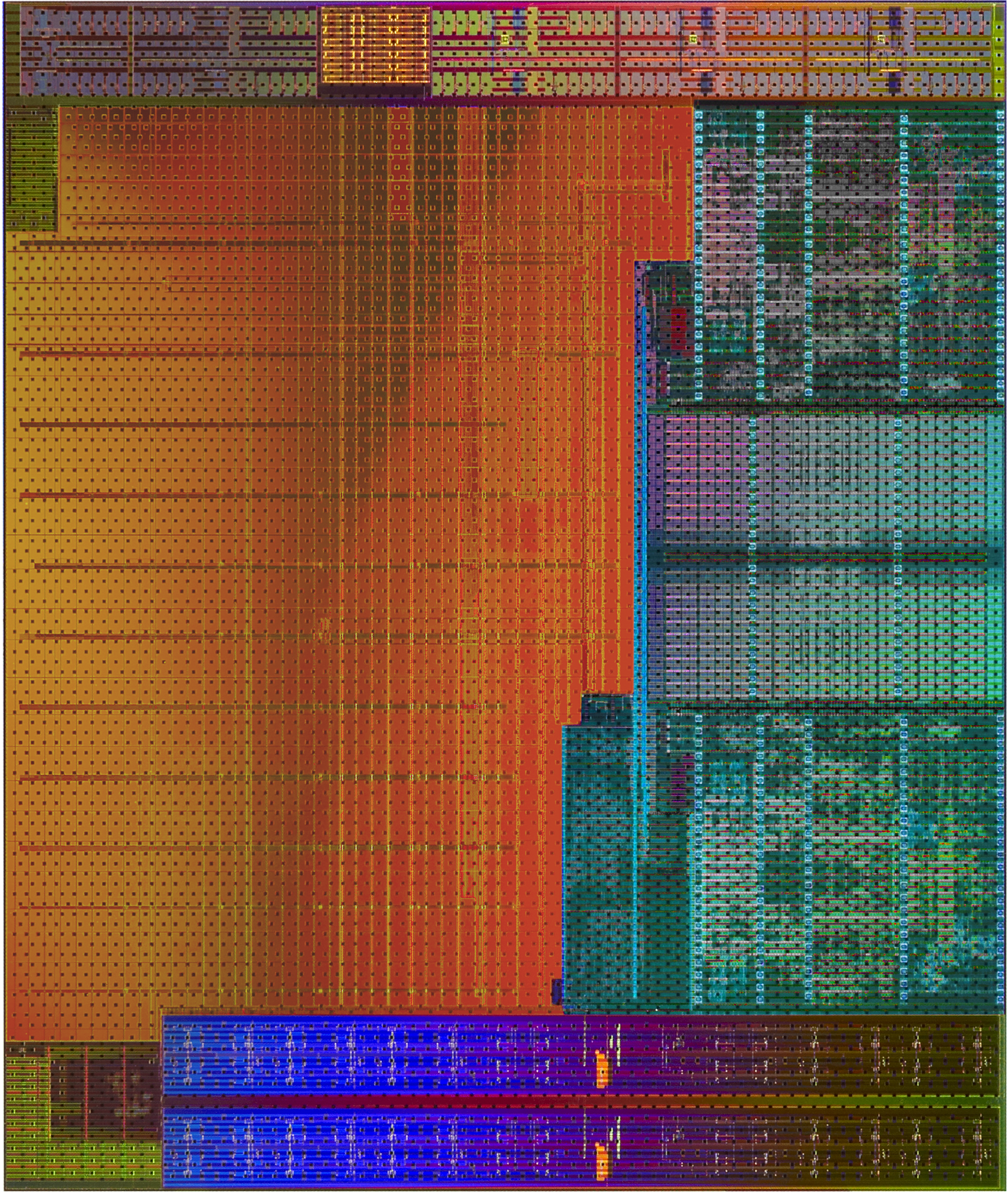
Trinity and Richland Die, with two Piledriver modules and processor graphics
Kaveri, two modules and processor graphics
Moving from Llano to Trinity, we have the reduction from a fully-fledged quad core system to the dual module layout AMD is keeping with its APU range. Moving from Richland to Kaveri is actually a bigger step than one might imagine:
| AMD APU Details | ||||
| Core Name | Llano | Trinity | Richland | Kaveri |
| Microarch | K10 | Piledriver | Piledriver | Steamroller |
| CPU Example | A8-3850 | A10-5800K | A10-6800K | A10-7850K |
| Threads | 4 | 4 | 4 | 4 |
| Cores | 4 | 2 | 2 | 2 |
| GPU | HD 6550 | HD 7660D | HD 8670D | R7 |
| GPU Arch | VLIW5 | VLIW4 | VLIW4 | GCN 1.1 |
| GPU Cores | 400 | 384 | 384 | 512 |
| Die size / mm2 | 228 | 246 | 246 | 245 |
| Transistors | 1.178 B | 1.303 B | 1.303 B | 2.41 B |
| Power | 100W | 100W | 100W | 95W |
| CPU MHz | 2900 | 3800 | 4100 | 3700 |
| CPU Turbo | N/A | 4200 | 4400 | 4000 |
| L1 Cache |
256KB C$ 256KB D$ |
128KB C$ 64KB D$ |
128KB C$ 64KB D$ |
192KB C$ 64KB D$ |
| L2 Cache | 4 x 1MB | 2 x 2 MB | 2 x 2 MB | 2 x 2 MB |
| Node | 32nm SOI | 32nm SOI | 32nm SOI | 28nm SHP |
| Memory | DDR-1866 | DDR-1866 | DDR-2133 | DDR-2133 |
Looking back at Llano and Trinity/Richland, it's very clear that AMD's APUs on GF's 32nm SOI process had a real issue with transistor density. The table below attempts to put everything in perspective but keep in mind that, outside of Intel, no one does a good job of documenting how they are counting (estimating) transistors. My only hope is AMD's transistor counting methods are consistent across CPU and GPU, although that alone may be wishful thinking:
| Transistor Density Comparison | ||||||||
| Manufacturing Process | Transistor Count | Die Size | Transistors per mm2 | |||||
| AMD Kaveri | GF 28nm SHP | 2.41B | 245 mm2 | 9.837M | ||||
| AMD Richland | GF 32nm SOI | 1.30B | 246 mm2 | 5.285M | ||||
| AMD Llano | GF 32nm SOI | 1.178B | 228 mm2 | 5.166M | ||||
| AMD Bonaire (R7 260X) | TSMC 28nm | 2.08B | 160 mm2 | 13.000M | ||||
| AMD Pitcairn (R7 270/270X) | TSMC 28nm | 2.80B | 212 mm2 | 13.209M | ||||
| AMD Vishera (FX-8350) | GF 32nm SOI | 1.2B | 315 mm2 | 3.810M | ||||
| Intel Haswell 4C (GT2) | Intel 22nm | 1.40B | 177 mm2 | 7.910M | ||||
| NVIDIA GK106 (GTX 660) | TSMC 28nm | 2.54B | 214 mm2 | 11.869M | ||||
If AMD is indeed counting the same way across APUs/GPUs, the move to Kaveri doesn't look all that extreme but rather a good point in between previous APUs and other AMD GCN GPUs. Compared to standalone CPU architectures from AMD, it's clear that the APUs are far more dense thanks to big portions of their die being occupied by a GPU.


380 Comments
View All Comments
ABR - Thursday, January 16, 2014 - link
Kind of funny to hear "Iris" mentioned here given that the SGI O2 was an early example of a workstation with HUMA back in the mid-90's. :) There was no such thing as GPGPU back then (it might have helped save SGI if there was), but it provided a big help for memory-intensive things like texture-mapping.vinayshivakumar - Thursday, January 16, 2014 - link
Why are the iGPU codenames mentioned in the CPU benchmark and the CPU is in brackets ?? What is the reason to mention the GPU at all in a CPU test ? To the untrained eye , it might look as is HD3000 is faster than the AMD R7... Which is obviously not true...vinayshivakumar - Thursday, January 16, 2014 - link
Am I missing something here , apart from a bias ?Th-z - Thursday, January 16, 2014 - link
I agree the labels can be misleading, in CPU benchmarks other than the second table "Agisoft PS v1.0 Mapping IGP" on page 10, all other are done with CPU only. Some tables got it right while some have iGPU names leading the labels and model names in the brackets. What should be in the brackets are iGPUs. Consistency in labelling is needed. It's probably not intentional, just a result of messing up the labels and get the review out ASAP.ryrynz - Thursday, January 16, 2014 - link
You should be listing the GPU first in the Winrar results. The GPU is obviously not important in this benchmark and really shouldn't be specified at all.sonofsanta - Thursday, January 16, 2014 - link
"...the benchmark follows Jenson Button in the McLaren who starts on the grid in 22nd place, with the field made up of 11 Williams cars, 5 Marussia and 5 Caterham in that order."You sure a 2013 McLaren could make it through that field? I reckon it'd still fail to make the podium.
HaryHr - Thursday, January 16, 2014 - link
What's the story with Iris Pro and huge difference between average FPS and minimum FPS?In BI performance test: 78 average and 6 minimum, quality test: 20 average and 1 minimum.
If this is happening during gameplay this makes game almost unplayable. AMDs lineup has much smaller variance.
It would be nice to see time frame tests.
synce - Thursday, January 16, 2014 - link
What a disappointment... I thought the 7850K would be the first rig I've built in years but it's barely an improvement over the 6800 and still no match for an i5 :(Rogatti - Thursday, January 16, 2014 - link
Drivers still immature ... I will wait to form an opinionSolMiester - Thursday, January 16, 2014 - link
WOW, looks to me that the A10 6800k is the better bang. I saw only 1 game where the R7 bettered the 6800K where any of them were playable....