Intel Demonstrates new 45nm Transistors and Conroe's Successor
by Anand Lal Shimpi on January 27, 2007 12:00 AM EST- Posted in
- CPUs
Conroe has a Son: Introducing Penryn
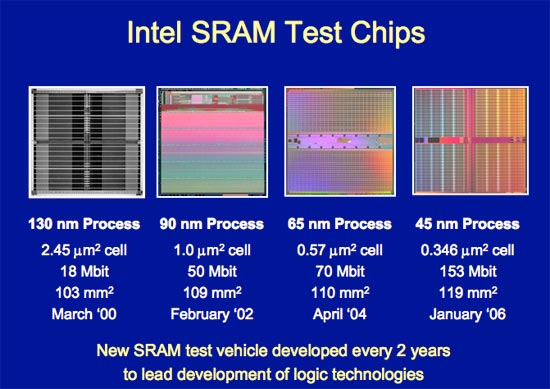
Intel announced the first working high-k + metal gate transistors back in 2003. By 2006 it had built an SRAM test vehicle (a wafer full of nothing but cache and some control/test logic) using the new transistors to work out most of the kinks in the manufacturing process.
Today, Intel is announcing that its first full CPU built using the new 45nm high-k + metal gate transistors is not only up and running, but it has also booted four OSes. The very first packaged Penryn silicon from the very first wafer booted Windows Vista, Mac OS X, Windows XP and Linux on the first try.
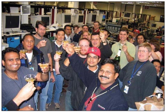
The picture below is of Intel's validation team after they successfully booted Penryn on the above OSes. The chips arrived in the lab at around 1AM and by 3AM they were up and running. If you're concerned, that's sparkling cider in those glasses and not champagne; alcohol is not allowed on Intel's campus, as it tends not to bring out the best in CPU designs, although it does make benchmark scores look infinitely higher.
It's a fairly big accomplishment to have first silicon working this well, but Intel has had a number of successful first spins in recent history. Generally by the time you're making your first CPUs, you've got the majority of the manufacturing defects worked out thanks to your SRAM test vehicle, so any problems with the first silicon are usually due to errors in the design or in the masks.
Intel also proudly sent us a shot of the 45nm Penryn die:
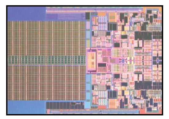
This version of Penryn is dual-core, and the first quad-core Penryn chips will simply be two of these on a single package, although later on we may see a single-die solution. At 410 million transistors, we expect a dual-core Penryn to have a 6MB shared L2 cache (up from 4MB in Conroe). The logic part of the Penryn core will be mostly evolutionary from Conroe, but do expect additional functionality and performance from more than just a larger cache.
If we assume that 288M transistors (6T SRAM) will be used by the 6MB cache, that leaves 122M transistors for L1 cache and the rest of the core. Applying the same calculation to Conroe gives us 99M transistors left over, meaning that there are roughly 23% more core-logic, control and L1 transistors being used in Penryn than in Conroe.
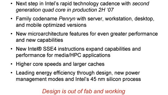
What that additional functionality will be is up in the air at this point, but you can expect SSE4 support to occupy a chunk of those transistors. At 45nm Intel should also be able to ramp up clock speed, so expect to see Penryn debut at over 3GHz easily. Given how overclockable Conroe turned out to be, we wouldn't be too surprised to see Penryn scale very well.
And the last bit of Penryn information Intel is letting out today is that it demonstrated Penryn up and running actual applications at a press briefing in Santa Clara on January 25th. There were five Penryn systems configured and clocked as follows:
1) 45nm dual core mobile processor in a notebook with Microsoft Vista running Microsoft Office 2003 applications.
2) 45nm dual-core desktop processor running high definition video content (1080P) under Microsoft Vista. 2.13 GHz
3) 45nm quad-core desktop processor running Ubisoft Rainbow Six Las Vegas game under Microsoft Vista. 1.86 GHz
4) Two 45nm dual-core processors running Glaze Workstation application under Microsoft Windows 2000 Advanced Server. 2.13 GHz
5) Two 45nm quad-core processors encoding a video in Adobe Premier under Microsoft Vista. 2.13 GHz
All of the systems were air-cooled using normal heatsink/fan units. Unfortunately Intel wouldn't share any benchmarks or more details of the systems other than what software they were running.
At this stage in the game it's normal to see clock speeds much lower than final shipping silicon, but this is the first time that Intel has been so forthcoming with clock speed data this far before launch. What we're seeing is a far more proud and confident Intel, and honestly it has every reason to be given the recent successes of Core 2 and promise of Penryn.


59 Comments
View All Comments
quidpro - Monday, February 26, 2007 - link
What is Glaze? google is not helping.Hoser McMoose - Wednesday, January 31, 2007 - link
The calculation for the number of transistors for cache is off by a fairly significant amount in this article! The article states 288M transistors for 6MB of cache, which is FAR too low!Actual transistors for 6MB cache, if we assume ZERO redundancy is:
6MB * 1024KB/MB * 1024B/KB = 6,291,456 bytes
6,291,456 bytes * 9 bits/byte = 56,623,104 bits (remember ECC makes it 9 bits, not 8)
56,623,104 bits * 6 bits/transistor ~= 340M transistors
In reality it is actually probably more like 350 or 360M transistors required for 6MB of L2 cache since you always want a bit of redundancy. It's a bad thing if you have to throw out an entire chip due to a single bit error in your 6MB of cache!
Now, taking those numbers, if we assume that the 410M Transistor figure is accurate, the change in transistors from Conroe to Penryn is a bit different.
Conroe has 291M transistors of which at least 226M are L2 cache. That leaves only 65M assuming no redundancy, or maybe more like 50M transistors with a few redundant cache cells. According to www.sandpile.org (and I have no idea what their source is) each core of the Core 2 Duo has only 19M logic transistors. If this is accurate then it's actually HUGELY impressive, since that is WAY less then either the Pentium 4 or the Athlon64.
Murst - Monday, January 29, 2007 - link
"Intel isn't disclosing how thick the Hafnium gate dielectric layer is in its 45nm transistors, but we do know that it is thicker than the 1.2nm SiO2 gate dielectric used in previous 90nm and 65nm transistors."Why would intel make the gate larger in a shrink? Is this a typo, or is there some huge benefit to this?
IntelUser2000 - Tuesday, January 30, 2007 - link
The reason is that making the gate dielectric thinner than 1.2nm is not a good idea. 1.2nm dielectric is already equivalent to 5 atoms in thickness. Electrons can literally squeeze through the dielectric "insulator" because the dielectric is so thin. Because the material used for the dielectric layer is different from the 65nm generation, they can make the dielectric thicker without sacrificing speed characteristics. So they can increase speed AND have substantially less leakage.
Visual - Monday, January 29, 2007 - link
So, I'm a bit out of the loop lately, can anyone brief me up?Are there any new sockets, chipsets, ram changes or anything expected together with these new 45nm goodies? Or will I be fine getting a new system come Q2, and upgrading to Penryn when it's out and affordable?
ceefka - Monday, January 29, 2007 - link
I wonder if booting OXS with the new chip indicates that PC-users can soon use OSX too without having to buy a Mac. That would allow to mix and match a bit more with apps.Netopia - Sunday, January 28, 2007 - link
100 * 100 =10,000
50 * 50 = 2,500
That's a 4x improvement, not a 2x!
Joe
coldpower27 - Sunday, January 28, 2007 - link
That is not how it works...65 x 65 = 4225
45 x 45 = 2025
2025/4225 = 48% the size of the 65nm part, so close to 2x smaller.
IntelUser2000 - Sunday, January 28, 2007 - link
That's the theory. Intel's 45nm 6T SRAM size is 0.346um, and 65nm SRAM cell size is 0.57um. That's only 39% reduction(61% of the size). In addition, SRAM, which is used for cache, has the best potential for scaling. The cores will have likely worse scaling than 61%.
coldpower27 - Monday, January 29, 2007 - link
Yes, I was just presenting the mathematical example of the calculation, I wasn't going into having real world factors involved. Since in this article Anandtech simplified things with just the 2x smaller statement.